- 您现在的位置:买卖IC网 > PDF目录80448 > MB9BF505NBGL 32-BIT, FLASH, 80 MHz, RISC MICROCONTROLLER, PBGA112 PDF资料下载
参数资料
| 型号: | MB9BF505NBGL |
| 元件分类: | 微控制器/微处理器 |
| 英文描述: | 32-BIT, FLASH, 80 MHz, RISC MICROCONTROLLER, PBGA112 |
| 封装: | 10 X 10 MM, 1.45 MM HEIGHT, 0.80 MM PITCH, PLASTIC, FBGA-112 |
| 文件页数: | 11/120页 |
| 文件大小: | 1277K |
| 代理商: | MB9BF505NBGL |
第1页第2页第3页第4页第5页第6页第7页第8页第9页第10页当前第11页第12页第13页第14页第15页第16页第17页第18页第19页第20页第21页第22页第23页第24页第25页第26页第27页第28页第29页第30页第31页第32页第33页第34页第35页第36页第37页第38页第39页第40页第41页第42页第43页第44页第45页第46页第47页第48页第49页第50页第51页第52页第53页第54页第55页第56页第57页第58页第59页第60页第61页第62页第63页第64页第65页第66页第67页第68页第69页第70页第71页第72页第73页第74页第75页第76页第77页第78页第79页第80页第81页第82页第83页第84页第85页第86页第87页第88页第89页第90页第91页第92页第93页第94页第95页第96页第97页第98页第99页第100页第101页第102页第103页第104页第105页第106页第107页第108页第109页第110页第111页第112页第113页第114页第115页第116页第117页第118页第119页第120页
108
8266D-MCU Wireless-06/12
ATmega128RFA1
Bit 7:0 – Res7:0 - Reserved
These bits are reserved for future use.
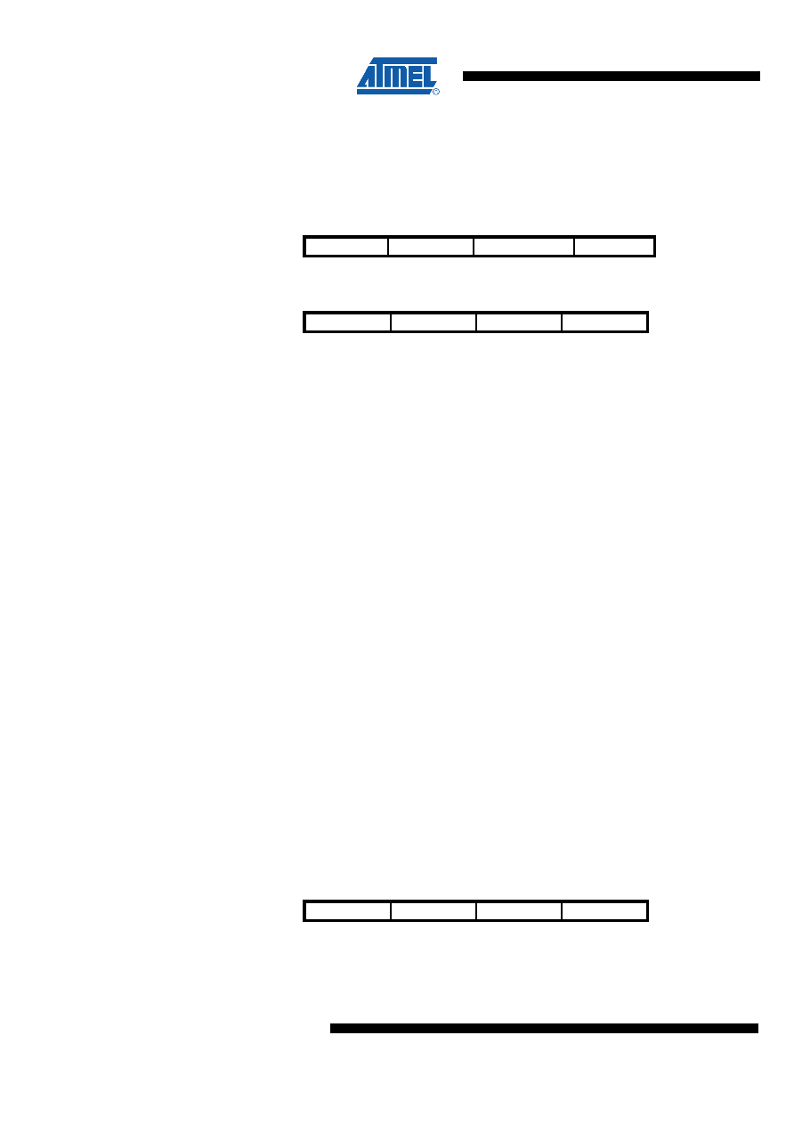
9.12.8 TRX_CTRL_1 – Transceiver Control Register 1
Bit
7
6
5
4
NA ($144)
PA_EXT_EN
IRQ_2_EXT_EN
TX_AUTO_CRC_ON
Res4
TRX_CTRL_1
Read/Write
RW
R
Initial Value
0
1
0
Bit
3
2
1
0
NA ($144)
Res3
Res2
Res1
Res0
TRX_CTRL_1
Read/Write
R
Initial Value
0
The TRX_CTRL_1 register is a multi purpose register to control various operating
modes and settings of the radio transceiver.
Bit 7 – PA_EXT_EN - External PA support enable
This register bit enables pin DIG3 and pin DIG4 to indicate the transmit state of the
radio transceiver. The control of the external RF front-end is disabled when this bit is 0.
Both pins DIG3 and DIG4 are then defined by the register of I/O ports F and G (PORTF,
DDRF, PORTG, DDRG). The control of the external front-end is enabled when this bit is
1. DIG3 and DIG4 then indicate the state of the radio transceiver. Pin DIG3 is high and
pin DIG4 is low in the state TX_BUSY. In all other states pin DIG3 is low and pin DIG4
is high. It is recommended to set PA_EXT_EN=1 only in receive or transmit states to
reduce the power consumption or avoid leakage current of external RF switches or
other building blocks especially during SLEEP state.
Bit 6 – IRQ_2_EXT_EN - Connect Frame Start IRQ to TC1
When this bit is set to one the capture input of Timer/Counter 1 is connected to the RX
frame start signal and pin DIG2 becomes an output, driving the RX frame start signal.
Antenna Diversity RF switch control (ANT_EXT_SW_EN=1) shall not be used at the
same time, because it shares the same device pin. The function IRQ_2_EXT_EN is
available for alternate frame time stamping using Timer/Counter 1. In general the
preferred method for frame time stamping is using the symbol counter.
Bit 5 – TX_AUTO_CRC_ON - Enable Automatic CRC Calculation
This register bit controls the automatic FCS generation for TX operations. The
automatic FCS algorithm is performed autonomously by the radio transceiver if register
bit TX_AUTO_CRC_ON=1.
Bit 4:0 – Res4:0 - Reserved
9.12.9 PHY_TX_PWR – Transceiver Transmit Power Control Register
Bit
7
6
5
4
NA ($145)
PA_BUF_LT1
PA_BUF_LT0
PA_LT1
PA_LT0
PHY_TX_PWR
Read/Write
RW
Initial Value
1
0
相关PDF资料 |
PDF描述 |
|---|---|
| MC68HC11ED0CFN2 | 8-BIT, 2 MHz, MICROCONTROLLER, PQCC44 |
| MSM80C31-JS | 8-BIT, 12 MHz, MICROCONTROLLER, PQCC44 |
| MSM80C50-RS | 8-BIT, MROM, 11 MHz, MICROCONTROLLER, PDIP40 |
| MSM83C154-1TS-K | 8-BIT, MROM, 16 MHz, MICROCONTROLLER, PQFP44 |
| MAB8032AH-2-15P | 8-BIT, 15 MHz, MICROCONTROLLER, PDIP40 |
相关代理商/技术参数 |
参数描述 |
|---|---|
| MB9BF506NABGL-GE1 | 制造商:FUJITSU 功能描述:MCU 32BIT CORTEX-M3 FM3 112BGA 制造商:FUJITSU 功能描述:MCU, 32BIT, CORTEX-M3, FM3, 112BGA, Controller Family/Series:ARM Cortex-M3, Core |
| MB9BF506NAPMC-G-JNE1 | 制造商:FUJITSU 功能描述: 制造商:FUJITSU 功能描述:MCU 32BIT CORTEX-M3 FM3 100LQFP 制造商:FUJITSU 功能描述:MCU, 32BIT, CORTEX-M3, FM3, 100LQFP 制造商:FUJITSU 功能描述:MCU, 32BIT, CORTEX-M3, FM3, 100LQFP, Controller Family/Series:ARM Cortex-M3, Core Size:32bit, No. of I/O's:80, Supply Voltage Min:2.7V, Supply Voltage Max:5.5V, Digital IC Case Style:LQFP, No. of Pins:100, Program Memory Size:512KB, , RoHS Compliant: Yes |
| MB9BF506NBBGL-GE1 | 制造商:FUJITSU 功能描述: |
| MB9BF506NBPMC-G-JNE2 | 制造商:FUJITSU 功能描述: |
| MB9BF506NPMC-ESE1 | 制造商:FUJITSU 功能描述: |
发布紧急采购,3分钟左右您将得到回复。