- 您现在的位置:买卖IC网 > PDF目录296481 > MBM29F017A-90PFTN (SPANSION LLC) 2M X 8 FLASH 5V PROM, 90 ns, PDSO48 PDF资料下载
参数资料
| 型号: | MBM29F017A-90PFTN |
| 厂商: | SPANSION LLC |
| 元件分类: | PROM |
| 英文描述: | 2M X 8 FLASH 5V PROM, 90 ns, PDSO48 |
| 封装: | PLASTIC, TSOP1-48 |
| 文件页数: | 16/49页 |
| 文件大小: | 520K |
| 代理商: | MBM29F017A-90PFTN |
第1页第2页第3页第4页第5页第6页第7页第8页第9页第10页第11页第12页第13页第14页第15页当前第16页第17页第18页第19页第20页第21页第22页第23页第24页第25页第26页第27页第28页第29页第30页第31页第32页第33页第34页第35页第36页第37页第38页第39页第40页第41页第42页第43页第44页第45页第46页第47页第48页第49页
MBM29F017A-70/-90/-12
22
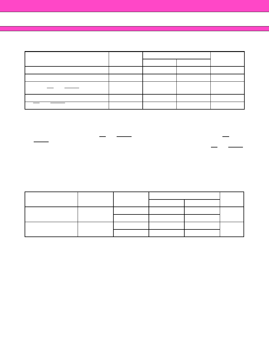
s ABSOLUTE MAXIMUM RATINGS
*1 : Voltage is defined on the basis of VSS
= GND = 0 V.
*2 : Minimum DC voltage on input or l/O pins is –0.5 V. During voltage transitions, input or I/O pins may undershoot
VSS to –2.0 V for periods of up to 20 ns. Maximum DC voltage on output and l/O pins is VCC +0.5 V. During voltage
transitions, outputs may overshoot to VCC +2.0 V for periods of up to 20 ns.
*3 : Minimum DC input voltage on A9, OE, and RESET pins are –0.5 V. During voltage transitions, A9, OE, and
RESET pins may undershoot VSS to –2.0 V for periods of up to 20 ns. Voltage difference between input and
power supply voltage (VIN
VCC) does not exceed +9.0 V. Maximum DC input voltage on A9, OE, and RESET
pins is
+13.0 V which may overshoot to +14.0 V for periods of up to 20 ns.
WARNING: Semiconductor devices can be permanently damaged by application of stress (voltage, current,
temperature, etc.) in excess of absolute maximum ratings. Do not exceed these ratings.
s RECOMMENDED OPERATING CONDITIONS
* : Voltage is defined on the basis of VSS
= GND = 0 V.
Note : Operating ranges define those limits between which the functionality of the device is guaranteed.
WARNING: The recommended operating conditions are required in order to ensure the normal operation of the
semiconductor device. All of the device’s electrical characteristics are warranted when the device is
operated within these ranges.
Always use semiconductor devices within their recommended operating condition ranges. Operation
outside these ranges may adversely affect reliability and could result in device failure.
No warranty is made with respect to uses, operating conditions, or combinations not represented on
the data sheet. Users considering application outside the listed conditions are advised to contact their
FUJITSU representatives beforehand.
Parameter
Symbol
Rating
Unit
Min
Max
Storage Temperature
Tstg
–55
+125
°C
Ambient Temperature with Power Applied
TA
–40
+85
°C
Voltage with respect to Ground All pins
except A9, OE, and RESET *1, *2
VIN, VOUT
–2.0
+7.0
V
Power Supply Voltage *1
VCC
–2.0
+7.0
V
A9, OE, and RESET *1, *3
VIN
–2.0
+13.5
V
Parameter
Symbol
Condition
Value
Unit
Min
Max
Ambient Temperature
TA
-70
–20
+70
°C
-90/-12
–40
+85
Power Supply Voltages *
VCC
-70
+4.75
+5.25
V
-90/-12
+4.50
+5.50
相关PDF资料 |
PDF描述 |
|---|---|
| MBM29LV160BE12PBT-E1 | 2M X 8 FLASH 3V PROM, 120 ns, PBGA48 |
| MBM29LV200B-10PFTR | 256K X 8 FLASH 3V PROM, 100 ns, PDSO48 |
| MBM29LV800BE70TN | 512K X 16 FLASH 3V PROM, 70 ns, PDSO48 |
| MBPL1319B-1R2-KS | 1 ELEMENT, 1.2 uH, GENERAL PURPOSE INDUCTOR |
| MBPL1319B-R30-KS | 1 ELEMENT, 0.3 uH, GENERAL PURPOSE INDUCTOR |
相关代理商/技术参数 |
参数描述 |
|---|---|
| MBM29F017A-90PFTR | 制造商:FUJITSU 制造商全称:Fujitsu Component Limited. 功能描述:16M (2M X 8) BIT |
| MBM29F017A-90PNS | 制造商:FUJITSU 制造商全称:Fujitsu Component Limited. 功能描述:16M (2M X 8) BIT |
| MBM29F033C | 制造商:FUJITSU 制造商全称:Fujitsu Component Limited. 功能描述:32M (4M X 8) BIT |
| MBM29F033C-12 | 制造商:FUJITSU 制造商全称:Fujitsu Component Limited. 功能描述:32M (4M X 8) BIT |
| MBM29F033C-12PTN | 制造商:FUJITSU 制造商全称:Fujitsu Component Limited. 功能描述:32M (4M X 8) BIT |
发布紧急采购,3分钟左右您将得到回复。