- 您现在的位置:买卖IC网 > PDF目录11718 > MC33560DTB (ON Semiconductor)OC PWR MGMT READERS/CPLR 24TSSOP PDF资料下载
参数资料
| 型号: | MC33560DTB |
| 厂商: | ON Semiconductor |
| 文件页数: | 8/26页 |
| 文件大小: | 0K |
| 描述: | OC PWR MGMT READERS/CPLR 24TSSOP |
| 标准包装: | 62 |
| 系列: | * |
| 应用: | * |
| 接口: | * |
| 电源电压: | * |
| 封装/外壳: | 24-TSSOP(0.220",5.60mm 宽) |
| 供应商设备封装: | 24-TSSOP |
| 包装: | 管件 |
| 安装类型: | 表面贴装 |
MC33560
http://onsemi.com
16
First, determine the maximum current that the application
requires to supply to the card (ICCmax, on the yaxis)
Then, select one curve that crosses the selected ICCmax
level. The curve is associated with an inductance value
(22
mH, 47 mH, or 100 mH).
Finally, use the intersection of the curve and the ICCmax
level to find the Rlim value on the xaxis.
Good starting values are : L1 = 47
mH; Rlim = 0.5 W
Note also that, for a high inductance value (100
mH), the
filtering capacitor is generally charged before inductance
current reaches current limitation, while for alow inductance
value, the current limitation is activated after a few converter
cycles.
Battery Requirements: Having determined the L1 and
Rlim values, the maximum current drawn from the battery
When the application is powered by a single 3.0 V battery,
special care has to be taken to extend its lifetime. When
lithium batteries approach the endoflife, their internal
resistance
increases,
while
voltage
decreases.
This
phenomenon can prevent the startup of the DCDC
converter if the current limiting is set too high, because of the
filtering capacitor charging current.
CLOCK GENERATOR
The primary purpose of the clock generator module is to
match the smartcard operating frequency to the system
frequency. The source frequency can be provided to
ASYCLKIN by the microcontroller itself or from an
external oscillator circuit.
In programming mode (RDYMOD=L and CS asserted
low) the three input variables PWRON, I/O and RESET are
used to configure the two output variables CRDVCC and
CRDCLK as described in Table 3. This circuit setup is
latched during the positive transition of CS.
Furthermore, in asynchronous mode the system clock
frequency ASYCLKIN can be divided by a factor of 1, 2
or 4. The circuit controls the frequency commutation to
guarantee that the card clock signal remains free from spikes
and glitches. In addition, this circuit ensures that CRDCLK
signal pulses will not be shorter than the shortest and/or
longer than the longest of the clock signals present before
and after programming changes.
The INVOUT output is provided to drive other circuits
without additional load to the microprocessor quartz
oscillator. It can also be used to build a local RC oscillator.
This driver has been optimized for low consumption; it has
no hysteresis, and input levels are not symmetrical. If the
ASYCLKIN pin is connected to a sine wave, the duty cycle
will not always be 50% at INVOUT.
CLOCK GENERATOR OPERATING PRINCIPLES
Synchronous Clock: This clock is used mainly for
memory cards. It can also be used for asynchronous
(microprocessor) cards, allowing the use of two different
clock sources. The status of SYNCLK is latched at
CRDCLK when CS goes high, so that data (the I/O pin) and
clock are always consistent at the card connector, whatever
the CS status is. When using the synchronous clock, the
clock output becomes active only when the MC33560 is
selected with CS.
Asynchronous Clock: This clock is used mainly for
microprocessor cards. When applied, the clock output
remains active even when the MC33560 is not selected with
CS, in order to keep the microprocessor running and avoid
an unwanted reset. The ASYCLKIN signal is buffered at the
INVOUT pin, so that several MC33560 systems can use the
same clock with one load only.
Depending on programming, the frequency is fed directly,
or divided by 2 or by 4 to the CRDCLK pin. If the duty cycle
of the applied clock signal is not exactly symmetrical, it is
recommended that the clock signal be divided by two or four
to guarantee 50% duty cycle.
Clock
Signal
Synchronization
and
Consistency
(Figure 29). The clock divider includes synchronization
logic that controls the switch from synchronous clock to
asynchronous (and viceversa), from any division ratio to
any other ratio, during CS changes and at powerup. The
synchronization logic guarantees that each clock cycle on
the CRDCLK pin is finished before changing clock
selection (and has always the adequate duration), regardless
of the moment the programming is changed.
At powerup, when ASYCLKIN is selected, the clock
signal at the CRDCLK pin has an entire length, according
to the selected divide ratio, whatever the ASYCLKIN signal
is versus the internal sequencer timing.
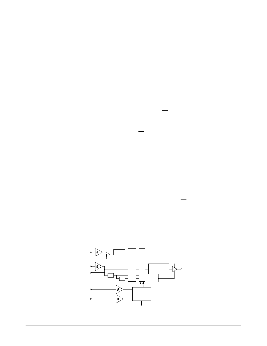
Figure 23. Clock Generator Functional Block
IO
RESET
SYNCLK
ASYCLKIN
INVOUT
CARDENABLE
SYNCHRONISA
TION
LOGIC
SELECT
OR
SELECTOR
LATCH
SYNCHRO
LATCH
CRDVCC
CRDCLK
SEQ3
PROGRAM
2
B
LATCH
2
B
相关PDF资料 |
PDF描述 |
|---|---|
| MC100E446FNR2 | IC CONV 4BIT SER/PAR ECL 28-PLCC |
| D38999/26WG41SN | CONN PLUG 41POS STRAIGHT W/SCKT |
| D38999/24JD18HN | CONN RCPT 18POS JAM NUT W/PINS |
| MCZ33797EK | IC SQUIB DRIVER 4-CH 32-SOIC |
| MCZ33889BEG | IC SYSTEM BASIS W/CAN 28-SOIC |
相关代理商/技术参数 |
参数描述 |
|---|---|
| MC33560DTBR2 | 功能描述:输入/输出控制器接口集成电路 3V/5V Smartcard RoHS:否 制造商:Silicon Labs 产品: 输入/输出端数量: 工作电源电压: 最大工作温度:+ 85 C 最小工作温度:- 40 C 安装风格:SMD/SMT 封装 / 箱体:QFN-64 封装:Tray |
| MC33560DTBR2G | 功能描述:输入/输出控制器接口集成电路 3V/5V Smartcard Power Management RoHS:否 制造商:Silicon Labs 产品: 输入/输出端数量: 工作电源电压: 最大工作温度:+ 85 C 最小工作温度:- 40 C 安装风格:SMD/SMT 封装 / 箱体:QFN-64 封装:Tray |
| MC33560DW | 功能描述:输入/输出控制器接口集成电路 3V/5V Smartcard RoHS:否 制造商:Silicon Labs 产品: 输入/输出端数量: 工作电源电压: 最大工作温度:+ 85 C 最小工作温度:- 40 C 安装风格:SMD/SMT 封装 / 箱体:QFN-64 封装:Tray |
| MC33560DWR2 | 功能描述:输入/输出控制器接口集成电路 3V/5V Smartcard RoHS:否 制造商:Silicon Labs 产品: 输入/输出端数量: 工作电源电压: 最大工作温度:+ 85 C 最小工作温度:- 40 C 安装风格:SMD/SMT 封装 / 箱体:QFN-64 封装:Tray |
| MC33560DWR2G | 功能描述:输入/输出控制器接口集成电路 3V/5V Smartcard Power Management RoHS:否 制造商:Silicon Labs 产品: 输入/输出端数量: 工作电源电压: 最大工作温度:+ 85 C 最小工作温度:- 40 C 安装风格:SMD/SMT 封装 / 箱体:QFN-64 封装:Tray |
发布紧急采购,3分钟左右您将得到回复。