- 您现在的位置:买卖IC网 > PDF目录16633 > MC33911BAC (Freescale Semiconductor)IC SYSTEM BASIS CHIP 32LQFP PDF资料下载
参数资料
| 型号: | MC33911BAC |
| 厂商: | Freescale Semiconductor |
| 文件页数: | 79/92页 |
| 文件大小: | 0K |
| 描述: | IC SYSTEM BASIS CHIP 32LQFP |
| 标准包装: | 250 |
| 应用: | 系统基础芯片 |
| 电流 - 电源: | 4.5mA |
| 电源电压: | 5.5 V ~ 27 V |
| 工作温度: | -40°C ~ 125°C |
| 安装类型: | 表面贴装 |
| 封装/外壳: | 32-LQFP |
| 供应商设备封装: | 32-LQFP(7x7) |
| 包装: | 托盘 |
第1页第2页第3页第4页第5页第6页第7页第8页第9页第10页第11页第12页第13页第14页第15页第16页第17页第18页第19页第20页第21页第22页第23页第24页第25页第26页第27页第28页第29页第30页第31页第32页第33页第34页第35页第36页第37页第38页第39页第40页第41页第42页第43页第44页第45页第46页第47页第48页第49页第50页第51页第52页第53页第54页第55页第56页第57页第58页第59页第60页第61页第62页第63页第64页第65页第66页第67页第68页第69页第70页第71页第72页第73页第74页第75页第76页第77页第78页当前第79页第80页第81页第82页第83页第84页第85页第86页第87页第88页第89页第90页第91页第92页
�� �
�
�MC33911BAC� /� MC34911BAC�
�FUNCTIONAL� DEVICE� OPERATIONS�
�LOGIC� COMMANDS� AND� REGISTERS�
�LOGIC� COMMANDS� AND� REGISTERS�
�33911� SPI� INTERFACE� AND� CONFIGURATION�
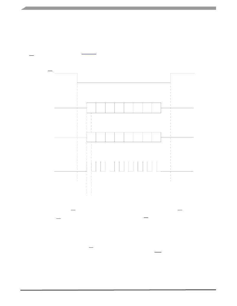
�The� serial� peripheral� interface� creates� the� communication�
�link� between� a� microcontroller� (master)� and� the� 33911.�
�The� interface� consists� of� four� pins� (see� Figure� 43� ):�
�?� CS� —� Chip� Select�
�?� MOSI� —� Master-Out� Slave-In�
�?� MISO� —� Master-In� Slave-Out�
�?� SCLK—� Serial� Clock�
�A� complete� data� transfer� via� the� SPI� consists� of� 1� byte.� The�
�master� sends� 4� bits� of� address� (A3:A0)� +� 4� bits� of� control�
�information� (C3:C0)� and� the� slave� replies� with� 4� system�
�status� bits� (VMS,LINS,HSS,LSS)� +� 4� bits� of� status�
�information� (S3:S0).�
�CS�
�Register� Write� Data�
�MOSI�
�A3�
�A2�
�A1�
�A0�
�C3�
�C2�
�C1�
�C0�
�Register� Read� Data�
�MISO�
�VMS� LINS� HSS�
�LSS�
�S3�
�S2�
�S1�
�S0�
�SCLK�
�Read� Data� Latch�
�Rising� Edge� of� SCLK�
�Change� MISO/MISO� Output�
�Falling� Edge� of� SCLK�
�Sample� MISO/MISO� Input�
�Figure� 43.� SPI� Protocol�
�Write� Data� Latch�
�During� the� inactive� phase� of� the� CS� (HIGH),� the� new� data�
�transfer� is� prepared.�
�The� falling� edge� of� the� CS� indicates� the� start� of� a� new� data�
�transfer� and� puts� the� MISO� in� the� low-impedance� state� and�
�latches� the� analog� status� data� (Register� read� data).�
�With� the� rising� edge� of� the� SPI� clock� (SCLK),� the� data� is�
�moved� to� MISO/MOSI� pins.� With� the� falling� edge� of� the� SPI�
�clock� (SCLK),� the� data� is� sampled� by� the� receiver.�
�The� data� transfer� is� only� valid� if� exactly� 8� sample� clock� edges�
�are� present� during� the� active� (low)� phase� of� CS� .�
�The� rising� edge� of� the� Chip� Select� (� CS)� indicates� the� end� of�
�the� transfer� and� latches� the� write� data� (MOSI)� into� the�
�register.� The� CS� high� forces� MISO� to� the� high-impedance�
�state.�
�Register� reset� values� are� described� along� with� the� reset�
�condition.� Reset� condition� is� the� condition� causing� the� bit� to�
�be� set� to� its� reset� value.� The� main� reset� conditions� are:�
�-� Power-On� Reset� (POR):� level� at� which� the� logic� is� reset� and�
�BATFAIL� flag� sets.�
�-� Reset� mode�
�-� Reset� done� by� the� RST� pin� (ext_reset)�
�33911�
�Analog� Integrated� Circuit� Device� Data� ?�
�79�
�Freescale� Semiconductor�
�相关PDF资料 |
PDF描述 |
|---|---|
| Q2-F-3/16-01-QX30FT | HEATSHRNK POLY Q2F 3/16" BLK 30' |
| 127R14-699B | CABLE FLAT FLEX 14POS 1.27MM 27. |
| 050R33-330B | CABLE FLAT FLEX 33POS .5MM 13" |
| RCM15DRYH-S13 | CONN EDGECARD 30POS .156 EXTEND |
| ABC05DRYN-S13 | CONN EDGECARD 10POS .100 EXTEND |
相关代理商/技术参数 |
参数描述 |
|---|---|
| MC33911BACR2 | 功能描述:LIN 收发器 SBC LIN2G MEDIUM END RoHS:否 制造商:NXP Semiconductors 工作电源电压: 电源电流: 最大工作温度: 封装 / 箱体:SO-8 |
| MC33911G5AC | 功能描述:LIN 收发器 SBC LIN 2.5G Medium end RoHS:否 制造商:NXP Semiconductors 工作电源电压: 电源电流: 最大工作温度: 封装 / 箱体:SO-8 |
| MC33911G5ACR2 | 功能描述:LIN 收发器 SBC LIN 2.5G Medium end RoHS:否 制造商:NXP Semiconductors 工作电源电压: 电源电流: 最大工作温度: 封装 / 箱体:SO-8 |
| MC33912BAC | 功能描述:LIN 收发器 SBC LIN2G - HI END RoHS:否 制造商:NXP Semiconductors 工作电源电压: 电源电流: 最大工作温度: 封装 / 箱体:SO-8 |
| MC33912BACR2 | 功能描述:LIN 收发器 SBC LIN2G - HI END RoHS:否 制造商:NXP Semiconductors 工作电源电压: 电源电流: 最大工作温度: 封装 / 箱体:SO-8 |
发布紧急采购,3分钟左右您将得到回复。