- 您现在的位置:买卖IC网 > PDF目录11546 > MC33989DW (Freescale Semiconductor)IC SYSTEM BASE W/CAN 28-SOIC PDF资料下载
参数资料
| 型号: | MC33989DW |
| 厂商: | Freescale Semiconductor |
| 文件页数: | 30/72页 |
| 文件大小: | 0K |
| 描述: | IC SYSTEM BASE W/CAN 28-SOIC |
| 标准包装: | 26 |
| 控制器类型: | 系统基础芯片 |
| 接口: | CAN |
| 电源电压: | 5.5 V ~ 18 V |
| 电流 - 电源: | 45mA |
| 工作温度: | -40°C ~ 125°C |
| 安装类型: | 表面贴装 |
| 封装/外壳: | 28-SOIC(0.295",7.50mm 宽) |
| 供应商设备封装: | 28-SOIC W |
| 包装: | 管件 |
| 配用: | KIT33989DWEVB-ND - KIT EVAL 33989DW HS SBC |
第1页第2页第3页第4页第5页第6页第7页第8页第9页第10页第11页第12页第13页第14页第15页第16页第17页第18页第19页第20页第21页第22页第23页第24页第25页第26页第27页第28页第29页当前第30页第31页第32页第33页第34页第35页第36页第37页第38页第39页第40页第41页第42页第43页第44页第45页第46页第47页第48页第49页第50页第51页第52页第53页第54页第55页第56页第57页第58页第59页第60页第61页第62页第63页第64页第65页第66页第67页第68页第69页第70页第71页第72页
Analog Integrated Circuit Device Data
36
Freescale Semiconductor
33989
FUNCTIONAL DEVICE OPERATION
LOGIC COMMANDS AND REGISTERS
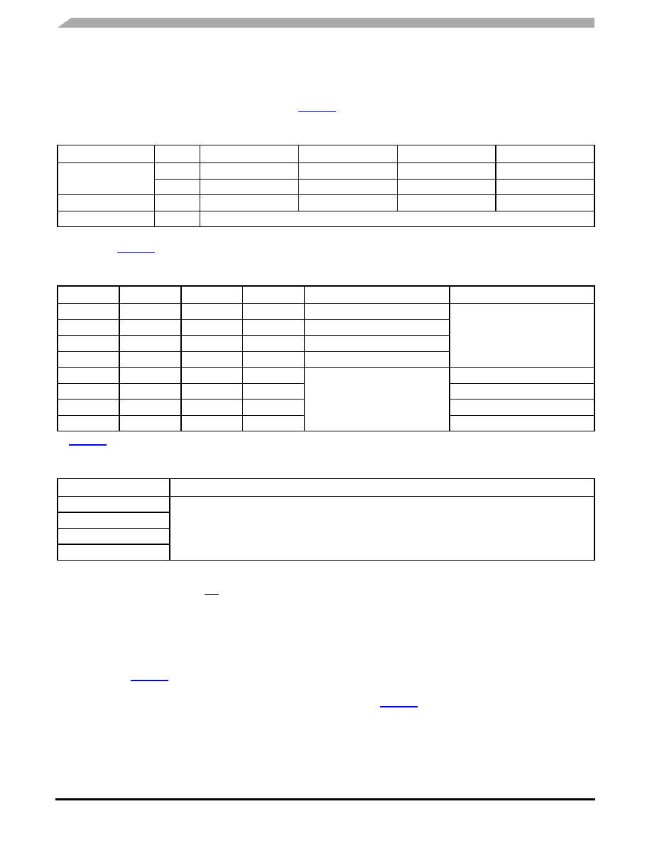
Wake-up Input Register (WUR)
The local wake-up inputs, L0, L1, L2, and L3 can be used in both Normal and Standby modes as port expander, as well as
and for waking up the SBC in Sleep or Stop modes. See Table 22.
The wake-up inputs can be configured separately, while L0 and L1 are configured together. Bits L2 and L3 are configured
together. See Table 23.
Table 24 provides Status bits data.
Timing Register (TIM1/2)
This register is composed of two registers:
1. TIM1–controls the watchdog timing selection as well as the window or timeout option. TIM1 is selected when bit D3 is 0.
Please see Table 25.
2. TIM2–is used to define the timing for the cyclic sense and forced wake-up function. TIM2 is selected when bit D3 is read
operation it is not allowed in either TIM1 or TIM2 registers. Please see Table 27.
Table 22. WUR Register
WUR
D3
D2
D1
D0
$100B
W
LCTR3
LCTR2
LCTR1
LCTR0
R
L3WU
L2WU
L1WU
L0WU
Reset Value
0
Reset Condition
POR, NR2R, N2R, STB2R, STO2R
Table 23. WUR Control Bits
LCTR3
LCTR2
LCTR1
LCTR0
L0/L1 Config
L2/L3 Config
x
0
Inputs Disabled
—
x
0
1
High Level Sensitive
x
1
0
Low Level Sensitive
x
1
Both Level Sensitive
0
x
—
Inputs Disabled
0
1
x
High Level Sensitive
1
0
x
Low Level Sensitive
1
x
Both Level Sensitive
Table 24. WUR Status Bits
Status Bit
Description
L3WU
Wake-up Occurred (Sleep/Stop Modes), Logic State on Lx (Standby/Normal Modes)
L2WU
L1WU
L0WU
Notes: Status bits have two functions. After SBC wake-up, they indicate the wake-up source (Example: L2WU set at 1 if wake-up source is L2
input). After SBC wake and once the WUR has been read, status bits indicates the real time state of the LX inputs (1 mean LX is above
threshold, 0 means that LX input is below threshold).
If, after a wake-up from LX input, a WD timeout occurs before the first reading of the WUR register, the LXxWU bits are reset. This can occur
only if SBC was in Stop mode.
相关PDF资料 |
PDF描述 |
|---|---|
| MC33889DW | IC SYSTEM BASE W/CAN 28-SOIC |
| MC33389CDW | IC SYSTEM BASE W/CAN 28-SOIC |
| MC33388DR2 | IC TOLERANT CAN INT FAULT 14SOIC |
| PX0414 | CONN SMB JACK PNL MNT RG174 |
| PIC16LF1937-E/PT | IC PIC MCU FLASH 512KX14 44-TQFP |
相关代理商/技术参数 |
参数描述 |
|---|---|
| MC33989DWR2 | 功能描述:CAN 接口集成电路 SBC HIGH SPEED RoHS:否 制造商:Texas Instruments 类型:Transceivers 工作电源电压:5 V 电源电流: 工作温度范围:- 40 C to + 85 C 封装 / 箱体:SOIC-8 封装:Tube |
| MC33989PEG | 功能描述:CAN 接口集成电路 SBC-HS RoHS:否 制造商:Texas Instruments 类型:Transceivers 工作电源电压:5 V 电源电流: 工作温度范围:- 40 C to + 85 C 封装 / 箱体:SOIC-8 封装:Tube |
| MC33989PEGR2 | 功能描述:CAN 接口集成电路 SBC-HS RoHS:否 制造商:Texas Instruments 类型:Transceivers 工作电源电压:5 V 电源电流: 工作温度范围:- 40 C to + 85 C 封装 / 箱体:SOIC-8 封装:Tube |
| MC33990D | 功能描述:IC TRANSCEIVER J-1850 BUS 8-SOIC RoHS:否 类别:集成电路 (IC) >> 接口 - 驱动器,接收器,收发器 系列:- 标准包装:1,000 系列:- 类型:收发器 驱动器/接收器数:2/2 规程:RS232 电源电压:3 V ~ 5.5 V 安装类型:表面贴装 封装/外壳:16-SOIC(0.295",7.50mm 宽) 供应商设备封装:16-SOIC 包装:带卷 (TR) |
| MC33990DR2 | 功能描述:IC TRANSCEIVER J-1850 BUS 8-SOIC RoHS:否 类别:集成电路 (IC) >> 接口 - 驱动器,接收器,收发器 系列:- 标准包装:1,000 系列:- 类型:收发器 驱动器/接收器数:2/2 规程:RS232 电源电压:3 V ~ 5.5 V 安装类型:表面贴装 封装/外壳:16-SOIC(0.295",7.50mm 宽) 供应商设备封装:16-SOIC 包装:带卷 (TR) |
发布紧急采购,3分钟左右您将得到回复。