- 您现在的位置:买卖IC网 > PDF目录16879 > MC35XS3500PNA (Freescale Semiconductor)IC SWITCH HIGHSIDE 24PQFN PDF资料下载
参数资料
| 型号: | MC35XS3500PNA |
| 厂商: | Freescale Semiconductor |
| 文件页数: | 22/45页 |
| 文件大小: | 0K |
| 描述: | IC SWITCH HIGHSIDE 24PQFN |
| 标准包装: | 168 |
| 类型: | 高端开关 |
| 输出数: | 5 |
| Rds(开): | * |
| 内部开关: | 是 |
| 电流限制: | 9A |
| 输入电压: | 7 V ~ 20 V |
| 工作温度: | -40°C ~ 125°C |
| 安装类型: | 表面贴装 |
| 封装/外壳: | 24-PowerQFN |
| 供应商设备封装: | 24-PQFN(12x12) |
| 包装: | 托盘 |
第1页第2页第3页第4页第5页第6页第7页第8页第9页第10页第11页第12页第13页第14页第15页第16页第17页第18页第19页第20页第21页当前第22页第23页第24页第25页第26页第27页第28页第29页第30页第31页第32页第33页第34页第35页第36页第37页第38页第39页第40页第41页第42页第43页第44页第45页
�� �
�
�FUNCTIONAL� DESCRIPTION�
�FUNCTIONAL� PIN� DESCRIPTION�
�CSB�
�SCLK�
�CS�
�SI�
�D15�
�D14�
�D13�
�D12�
�D11�
�D10�
�D9�
�D8�
�D7�
�D6�
�D5�
�D4�
�D3�
�D2�
�D1�
�D0�
�SO�
�OD15� OD14� OD13� OD12� OD11� OD10� OD9�
�OD8�
�OD7�
�OD6�
�OD5�
�OD4�
�OD3�
�OD2�
�OD1� OD0�
�1.� D15:D0� relate� to� the� most� recent� operation.� entry� of� data� into� the� device.�
�ordered�
�2.� OD15:OD0� and� D15� relate� to� first� most� bits� of� ordered� entry� fault� program� status� into� the� LUX� of� the� device.�
�DO,� D1,� D2,� ...� ,� relate� to� the� the� 16� recent� ordered�
�of� and� data� data� out� IC�
�Notes�
�NOTES:� 1.�
�2.�
�3�
�Serial� Input� (SI)�
�RSTB� is� in� a� logic� H� state� during� the� above�
�device.�
�LUX� IC�
�OD0� OD1� OD2� and� OD15� relate� to� the� first� 16� bits� of� ordered� fault� and� status� data� out� of� the� device.�
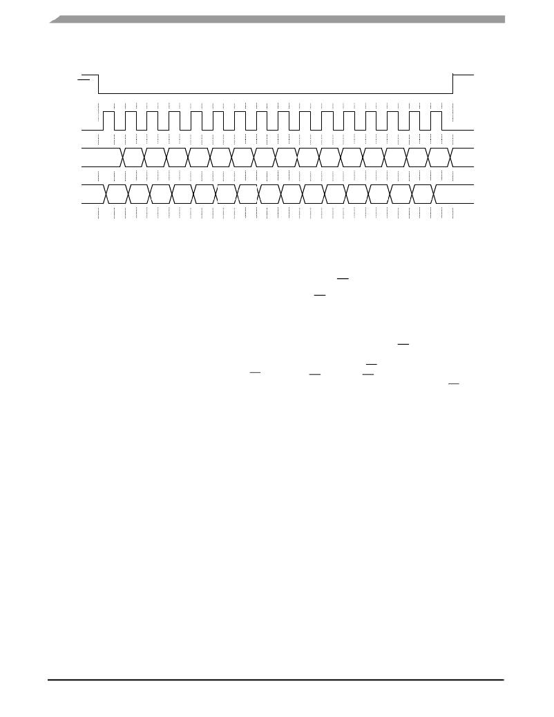
�Figure� 8.� Single� 16-Bit� Word� SPI� Communication�
�Chip� Select� (CS)�
�The� SI� pin� is� a� serial� interface� command� data� input� pin.�
�Each� SI� bit� is� read� on� the� falling� edge� of� SCLK.� A� 16-bit�
�stream� of� serial� data� is� required� on� the� SI� pin,� starting� with�
�D15� to� D0.� SI� has� a� passive� pull-down,� R� DOWN� .�
�Serial� Output� (SO)�
�The� SO� data� pin� is� a� tri-state� output� from� the� shift� register.�
�The� SO� pin� remains� in� a� high-impedance� state� until� the� CS�
�pin� is� put� into� a� logic� [0]� state.� The� SO� data� is� capable� of�
�reporting� the� status� of� the� output,� the� device� configuration,�
�and� the� state� of� the� key� inputs.� The� SO� pin� changes� state� on�
�the� rising� edge� of� SCLK� and� reads� out� on� the� falling� edge� of�
�SCLK.�
�The� CS� pin� enables� communication� with� the� master�
�device.� When� this� pin� is� in� a� logic� [0]� state,� the� device� is�
�capable� of� transferring� information� to,� and� receiving�
�information� from,� the� master� device.� The� 35XS3500� device�
�latches� in� data� from� the� Input� Shift� registers� to� the� addressed�
�registers� on� the� rising� edge� of� CS.� The� device� transfers�
�status� information� from� the� power� output� to� the� Shift� register�
�on� the� falling� edge� of� CS.� The� SO� output� driver� is� enabled�
�when� CS� is� logic� [0].� CS� should� transition� from� a� logic� [1]� to� a�
�logic� [0]� state� only� when� SCLK� is� a� logic� [0].� CS� has� a�
�passive� pull-up,� R� UP� .�
�STOP� Input� (STOP)�
�The� STOP� input� wakes� the� device.� It� also� controls� the� Fail�
�mode� activation.� The� signal� is� “high� active“,� meaning� the�
�component� is� active� in� case� of� a� logic� high� at� the� input.�
�35XS3500�
�Analog� Integrated� Circuit� Device� Data� ?�
�22�
�Freescale� Semiconductor�
�相关PDF资料 |
PDF描述 |
|---|---|
| GCC25DCMD-S288 | CONN EDGECARD 50POS .100 EXTEND |
| 342A124-4/42-0 | BOOT MOLDED |
| TCMD-17-D-02.00-01 | CABLE ASSEM 2MM 34POS M-M 2" |
| MC10XS3535PNAR2 | IC SWITCH HIGHSIDE 24PQFN |
| EBC31DCSN-S288 | CONN EDGECARD 62POS .100 EXTEND |
相关代理商/技术参数 |
参数描述 |
|---|---|
| MC35XS3500PNAR2 | 功能描述:功率驱动器IC 5 OUTPUT ESWITCH RoHS:否 制造商:Micrel 产品:MOSFET Gate Drivers 类型:Low Cost High or Low Side MOSFET Driver 上升时间: 下降时间: 电源电压-最大:30 V 电源电压-最小:2.75 V 电源电流: 最大功率耗散: 最大工作温度:+ 85 C 安装风格:SMD/SMT 封装 / 箱体:SOIC-8 封装:Tube |
| MC36089 | 制造商:SPC Multicomp 功能描述:ESD OPEN BIN BOX; ESD Storage Type:Bin; External Depth - Imperial:24.75"; External Depth - Metric:628.65mm; External Height - Imperial:4.5"; External Height - Metric:114.3mm; External Width - Imperial:4.25"; External Depth:24-3/4" ;RoHS Compliant: NA |
| MC36090 | 制造商:SPC Multicomp 功能描述:ESD OPEN BIN BOX; ESD Storage Type:Bin; External Depth - Imperial:24.75"; External Depth - Metric:628.65mm; External Height - Imperial:4.5"; External Height - Metric:114.3mm; External Width - Imperial:2.25"; External Depth:24-3/4" ;RoHS Compliant: NA |
| MC36091 | 制造商:SPC Multicomp 功能描述:ESD OPEN BIN BOX; ESD Storage Type:Bin; External Depth - Imperial:18"; External Depth - Metric:457.2mm; External Height - Imperial:4.5"; External Height - Metric:114.3mm; External Width - Imperial:4"; External Width - Metric:101.6mm ;RoHS Compliant: NA |
| MC36092 | 制造商:SPC Multicomp 功能描述:ESD OPEN BIN BOX; ESD Storage Type:Bin; External Depth - Imperial:18"; External Depth - Metric:457.2mm; External Height - Imperial:4.5"; External Height - Metric:114.3mm; External Width - Imperial:2"; External Width - Metric:50.8mm ;RoHS Compliant: NA |
发布紧急采购,3分钟左右您将得到回复。