- 您现在的位置:买卖IC网 > PDF目录132989 > MC56F8013VFAER2 (FREESCALE SEMICONDUCTOR INC) 0-BIT, 8 MHz, OTHER DSP, PQFP32 PDF资料下载
参数资料
| 型号: | MC56F8013VFAER2 |
| 厂商: | FREESCALE SEMICONDUCTOR INC |
| 元件分类: | 数字信号处理 |
| 英文描述: | 0-BIT, 8 MHz, OTHER DSP, PQFP32 |
| 封装: | ROHS COMPLIANT, LQFP-32 |
| 文件页数: | 103/125页 |
| 文件大小: | 1702K |
| 代理商: | MC56F8013VFAER2 |
第1页第2页第3页第4页第5页第6页第7页第8页第9页第10页第11页第12页第13页第14页第15页第16页第17页第18页第19页第20页第21页第22页第23页第24页第25页第26页第27页第28页第29页第30页第31页第32页第33页第34页第35页第36页第37页第38页第39页第40页第41页第42页第43页第44页第45页第46页第47页第48页第49页第50页第51页第52页第53页第54页第55页第56页第57页第58页第59页第60页第61页第62页第63页第64页第65页第66页第67页第68页第69页第70页第71页第72页第73页第74页第75页第76页第77页第78页第79页第80页第81页第82页第83页第84页第85页第86页第87页第88页第89页第90页第91页第92页第93页第94页第95页第96页第97页第98页第99页第100页第101页第102页当前第103页第104页第105页第106页第107页第108页第109页第110页第111页第112页第113页第114页第115页第116页第117页第118页第119页第120页第121页第122页第123页第124页第125页
Clock Generation Overview
56F8013/56F8011 Data Sheet, Rev. 11
Freescale Semiconductor
79
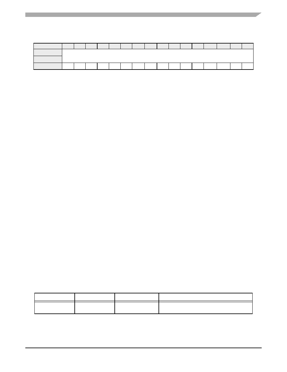
Figure 6-14 I/O Short Address Location Low Register (SIM_IOSALO)
6.3.10.3
Input/Output Short Address Location (ISAL[21:6])—Bits 15–0
This field represents the lower 16 address bits of the “hard coded” I/O short address.
6.4 Clock Generation Overview
The SIM uses master clocks, 2X system clock at a maximum of 64MHz, from the OCCS module to
produce the peripheral and system (core and memory) clocks at a maximum of 32MHz. It divides the
master clock by two and gates it with appropriate power mode and clock gating controls. The high speed
peripheral clock from OCCS operates at three times the system clock for PWM and Quad Timer module
at a maximum of 96MHz.
The OCCS configuration controls the operating frequency of the SIM’s master clocks. In the OCCS, either
an external clock or the relaxation oscillator can be selected as the master clock source (MSTR_OSC). The
relaxation oscillator can be operated at full speed (8MHz), standby speed (200kHz), or powered down. An
8MHz clock can be multiplied to 196MHz using the PLL and postscaled to provide a variety of high speed
clock rates. Either the postscaled PLL output or input clock of PLL signal can be selected to produce the
master clocks to the SIM. When the PLL is not selected, the high speed peripheral clock is disabled and
the 2X system clock is input clock from either internal relaxation oscillator or external clock source.
In combination with the OCCS module, the SIM provides power modes (see Section 6.5), clock enables
(SIM_PCE register, CLK_DIS, ONCE_EBL), and clock rate controls (TCR, PCR) to provide flexible
control of clocking and power utilization. The SIM’s clock enable controls can be used to disable
individual clocks when not needed. The clock rate controls enable the high speed clocking option for the
Timer channels and PWM but require the PLL to be on and selected. Refer to the 56F801X Peripheral
User Manual for further details.
6.5 Power-Down Modes
The 56F8013/56F8011 operates in one of five Power-Down modes, as shown in Table 6-3
Base + $E
15
14
13
12
11
10
9
8
7
6
5
4
3
2
1
0
Read
ISAL[21:6]
Write
RESET
11111
1
Table 6-3 Clock Operation in Power-Down Modes
Mode
Core Clocks
Peripheral Clocks
Description
Run
Core and memory
clocks disabled
Peripheral clocks
enabled
Device is fully functional
相关PDF资料 |
PDF描述 |
|---|---|
| MCIMX31VKN5BR2 | 532 MHz, MICROPROCESSOR, PBGA457 |
| MK5811CMLF | 32 MHz, OTHER CLOCK GENERATOR, PDSO8 |
| MCIMX27VJP4A | 32-BIT, 400 MHz, MICROPROCESSOR, PBGA404 |
| MCF52212AE50 | 32-BIT, FLASH, 50 MHz, RISC MICROCONTROLLER, PQFP64 |
| MB95F104AJSPMC | 16-BIT, FLASH, 16.25 MHz, RISC MICROCONTROLLER, PQFP64 |
相关代理商/技术参数 |
参数描述 |
|---|---|
| MC56F8014 | 制造商:FREESCALE 制造商全称:Freescale Semiconductor, Inc 功能描述:16-bit Digital Signal Controllers |
| MC56F8014E | 制造商:FREESCALE 制造商全称:Freescale Semiconductor, Inc 功能描述:16-bit Digital Signal Controllers |
| MC56F8014MFAE | 功能描述:数字信号处理器和控制器 - DSP, DSC 16Bit DSPHC RoHS:否 制造商:Microchip Technology 核心:dsPIC 数据总线宽度:16 bit 程序存储器大小:16 KB 数据 RAM 大小:2 KB 最大时钟频率:40 MHz 可编程输入/输出端数量:35 定时器数量:3 设备每秒兆指令数:50 MIPs 工作电源电压:3.3 V 最大工作温度:+ 85 C 封装 / 箱体:TQFP-44 安装风格:SMD/SMT |
| MC56F8014VFAE | 功能描述:数字信号处理器和控制器 - DSP, DSC 16 BIT DSPHC BAHAMAS RoHS:否 制造商:Microchip Technology 核心:dsPIC 数据总线宽度:16 bit 程序存储器大小:16 KB 数据 RAM 大小:2 KB 最大时钟频率:40 MHz 可编程输入/输出端数量:35 定时器数量:3 设备每秒兆指令数:50 MIPs 工作电源电压:3.3 V 最大工作温度:+ 85 C 封装 / 箱体:TQFP-44 安装风格:SMD/SMT |
| MC56F8023 | 制造商:FREESCALE 制造商全称:Freescale Semiconductor, Inc 功能描述:16-bit Digital Signal Controllers |
发布紧急采购,3分钟左右您将得到回复。