- 您现在的位置:买卖IC网 > PDF目录80565 > MC56F8346MFV60 (FREESCALE SEMICONDUCTOR INC) 16-BIT, 120 MHz, OTHER DSP, PQFP144 PDF资料下载
参数资料
| 型号: | MC56F8346MFV60 |
| 厂商: | FREESCALE SEMICONDUCTOR INC |
| 元件分类: | 数字信号处理 |
| 英文描述: | 16-BIT, 120 MHz, OTHER DSP, PQFP144 |
| 封装: | LQFP-144 |
| 文件页数: | 111/178页 |
| 文件大小: | 880K |
| 代理商: | MC56F8346MFV60 |
第1页第2页第3页第4页第5页第6页第7页第8页第9页第10页第11页第12页第13页第14页第15页第16页第17页第18页第19页第20页第21页第22页第23页第24页第25页第26页第27页第28页第29页第30页第31页第32页第33页第34页第35页第36页第37页第38页第39页第40页第41页第42页第43页第44页第45页第46页第47页第48页第49页第50页第51页第52页第53页第54页第55页第56页第57页第58页第59页第60页第61页第62页第63页第64页第65页第66页第67页第68页第69页第70页第71页第72页第73页第74页第75页第76页第77页第78页第79页第80页第81页第82页第83页第84页第85页第86页第87页第88页第89页第90页第91页第92页第93页第94页第95页第96页第97页第98页第99页第100页第101页第102页第103页第104页第105页第106页第107页第108页第109页第110页当前第111页第112页第113页第114页第115页第116页第117页第118页第119页第120页第121页第122页第123页第124页第125页第126页第127页第128页第129页第130页第131页第132页第133页第134页第135页第136页第137页第138页第139页第140页第141页第142页第143页第144页第145页第146页第147页第148页第149页第150页第151页第152页第153页第154页第155页第156页第157页第158页第159页第160页第161页第162页第163页第164页第165页第166页第167页第168页第169页第170页第171页第172页第173页第174页第175页第176页第177页第178页
56F8346 Technical Data, Rev. 15
38
Freescale Semiconductor
Preliminary
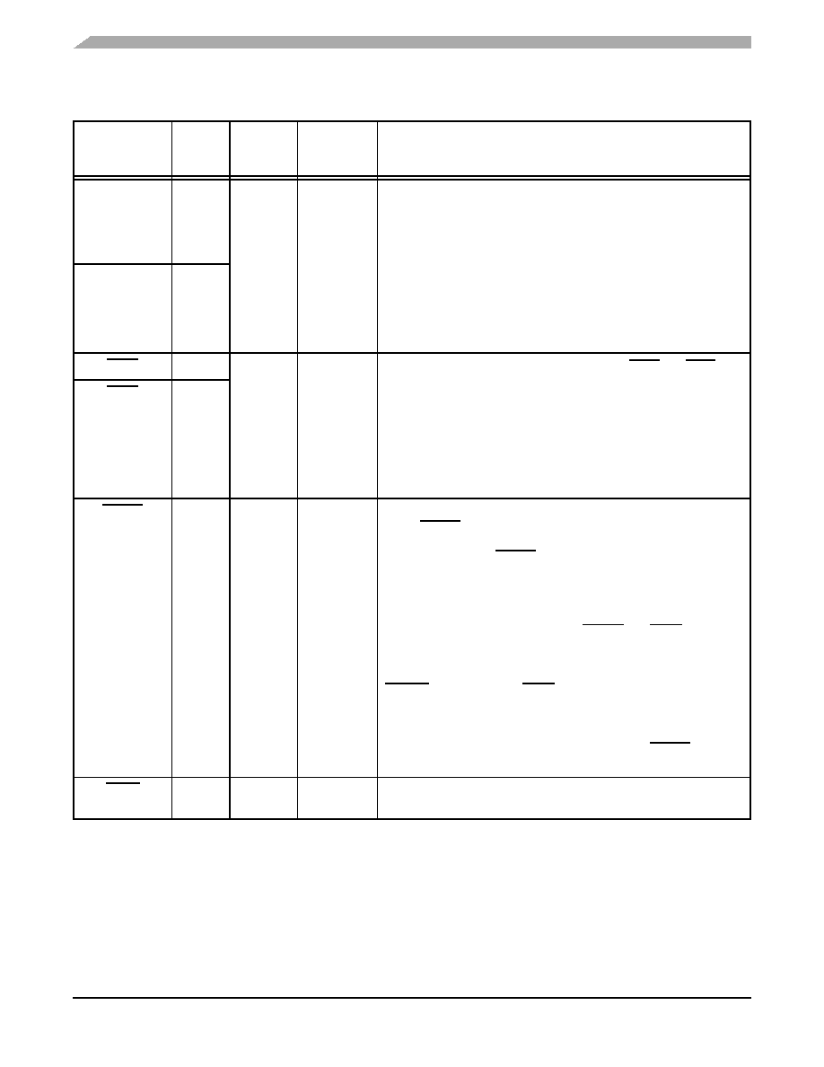
TD0
(GPIOE10)
116
Schmitt
Input/
Output
Schmitt
Input/
Output
Input,
pull-up
enabled
TD0 -1 — Timer D, Channels 0 and 1
Port E GPIO — These GPIO pins can be individually programmed
as input or output pins.
At reset, these pins default to Timer functionality.
To deactivate the internal pull-up resistor, clear the appropriate bit
of the GPIOE_PUR register. See Part 6.5.6 for details.
TD1
(GPIOE11)
117
IRQA
54
Schmitt
Input
Input,
pull-up
enabled
External Interrupt Request A and B — The IRQA and IRQB
inputs are asynchronous external interrupt requests during Stop
and Wait mode operation. During other operating modes, they are
synchronized external interrupt requests, which indicate an
external device is requesting service. They can be programmed to
be level-sensitive or negative-edge triggered.
To deactivate the internal pull-up resistor, set the IRQ bit in the
SIM_PUDR register. See Part 6.5.6 for details.
IRQB
55
RESET
86
Schmitt
Input
Input,
pull-up
enabled
Reset — This input is a direct hardware reset on the processor.
When RESET is asserted low, the device is initialized and placed
in the reset state. A Schmitt trigger input is used for noise
immunity. When the RESET pin is deasserted, the initial chip
operating mode is latched from the EXTBOOT pin. The internal
reset signal will be deasserted synchronous with the internal clocks
after a fixed number of internal clocks.
To ensure complete hardware reset, RESET and TRST should be
asserted together. The only exception occurs in a debugging
environment when a hardware device reset is required and the
JTAG/EOnCE module must not be reset. In this case, assert
RESET but do not assert TRST.
Note: The internal Power-On Reset will assert on initial power-up.
To deactivate the internal pull-up resistor, set the RESET bit in the
SIM_PUDR register. See Part 6.5.6 for details.
RSTO
85
Output
Reset Output — This output reflects the internal reset state of the
chip.
Table 2-2 Signal and Package Information for the 144 Pin LQFP
Signal Name
Pin No.
Type
State
During
Reset
Signal Description
相关PDF资料 |
PDF描述 |
|---|---|
| MC68020RP25 | 32-BIT, 25 MHz, MICROPROCESSOR, PPGA114 |
| MC9328MX1DVH20 | 200 MHz, RISC PROCESSOR, PBGA256 |
| MC68HC705J1AVDW | 8-BIT, OTPROM, 2.1 MHz, MICROCONTROLLER, PDSO20 |
| MC68HC908EY16MFA | 8-BIT, FLASH, 8 MHz, MICROCONTROLLER, PQFP32 |
| MC68HSR705J1AP | 8-BIT, OTPROM, MICROCONTROLLER, PDIP20 |
相关代理商/技术参数 |
参数描述 |
|---|---|
| MC56F8346MFVE | 功能描述:数字信号处理器和控制器 - DSP, DSC 16 BIT HYBRID CONTROLLER RoHS:否 制造商:Microchip Technology 核心:dsPIC 数据总线宽度:16 bit 程序存储器大小:16 KB 数据 RAM 大小:2 KB 最大时钟频率:40 MHz 可编程输入/输出端数量:35 定时器数量:3 设备每秒兆指令数:50 MIPs 工作电源电压:3.3 V 最大工作温度:+ 85 C 封装 / 箱体:TQFP-44 安装风格:SMD/SMT |
| MC56F8346VFV60 | 功能描述:数字信号处理器和控制器 - DSP, DSC 60MHz 60MIPS RoHS:否 制造商:Microchip Technology 核心:dsPIC 数据总线宽度:16 bit 程序存储器大小:16 KB 数据 RAM 大小:2 KB 最大时钟频率:40 MHz 可编程输入/输出端数量:35 定时器数量:3 设备每秒兆指令数:50 MIPs 工作电源电压:3.3 V 最大工作温度:+ 85 C 封装 / 箱体:TQFP-44 安装风格:SMD/SMT |
| MC56F8346VFVE | 功能描述:数字信号处理器和控制器 - DSP, DSC 16 BIT HYBRID CNTRLR RoHS:否 制造商:Microchip Technology 核心:dsPIC 数据总线宽度:16 bit 程序存储器大小:16 KB 数据 RAM 大小:2 KB 最大时钟频率:40 MHz 可编程输入/输出端数量:35 定时器数量:3 设备每秒兆指令数:50 MIPs 工作电源电压:3.3 V 最大工作温度:+ 85 C 封装 / 箱体:TQFP-44 安装风格:SMD/SMT |
| MC56F8346VFVER2 | 功能描述:数字信号处理器和控制器 - DSP, DSC 16 BIT HYBRID CNTRLR RoHS:否 制造商:Microchip Technology 核心:dsPIC 数据总线宽度:16 bit 程序存储器大小:16 KB 数据 RAM 大小:2 KB 最大时钟频率:40 MHz 可编程输入/输出端数量:35 定时器数量:3 设备每秒兆指令数:50 MIPs 工作电源电压:3.3 V 最大工作温度:+ 85 C 封装 / 箱体:TQFP-44 安装风格:SMD/SMT |
| MC56F8347 | 制造商:FREESCALE 制造商全称:Freescale Semiconductor, Inc 功能描述:16-bit Digital Signal Controllers |
发布紧急采购,3分钟左右您将得到回复。