- 您现在的位置:买卖IC网 > PDF目录80565 > MC56F8346MFV60 (FREESCALE SEMICONDUCTOR INC) 16-BIT, 120 MHz, OTHER DSP, PQFP144 PDF资料下载
参数资料
| 型号: | MC56F8346MFV60 |
| 厂商: | FREESCALE SEMICONDUCTOR INC |
| 元件分类: | 数字信号处理 |
| 英文描述: | 16-BIT, 120 MHz, OTHER DSP, PQFP144 |
| 封装: | LQFP-144 |
| 文件页数: | 54/178页 |
| 文件大小: | 880K |
| 代理商: | MC56F8346MFV60 |
第1页第2页第3页第4页第5页第6页第7页第8页第9页第10页第11页第12页第13页第14页第15页第16页第17页第18页第19页第20页第21页第22页第23页第24页第25页第26页第27页第28页第29页第30页第31页第32页第33页第34页第35页第36页第37页第38页第39页第40页第41页第42页第43页第44页第45页第46页第47页第48页第49页第50页第51页第52页第53页当前第54页第55页第56页第57页第58页第59页第60页第61页第62页第63页第64页第65页第66页第67页第68页第69页第70页第71页第72页第73页第74页第75页第76页第77页第78页第79页第80页第81页第82页第83页第84页第85页第86页第87页第88页第89页第90页第91页第92页第93页第94页第95页第96页第97页第98页第99页第100页第101页第102页第103页第104页第105页第106页第107页第108页第109页第110页第111页第112页第113页第114页第115页第116页第117页第118页第119页第120页第121页第122页第123页第124页第125页第126页第127页第128页第129页第130页第131页第132页第133页第134页第135页第136页第137页第138页第139页第140页第141页第142页第143页第144页第145页第146页第147页第148页第149页第150页第151页第152页第153页第154页第155页第156页第157页第158页第159页第160页第161页第162页第163页第164页第165页第166页第167页第168页第169页第170页第171页第172页第173页第174页第175页第176页第177页第178页
Crystal Oscillator Timing
56F8346 Technical Data, Rev. 15
Freescale Semiconductor
147
Preliminary
10.7 Crystal Oscillator Timing
10.8 External Memory Interface Timing
The External Memory Interface is designed to access static memory and peripheral devices. Figure 10-4
shows sample timing and parameters that are detailed in Table 10-16.
The timing of each parameter consists of both a fixed delay portion and a clock related portion, as well as
user controlled wait states. The equation:
t = D + P * (M + W)
should be used to determine the actual time of each parameter. The terms in this equation are defined as:
When using the XTAL clock input directly as the chip clock without prescaling (ZSRC selects prescaler
clock and prescaler is set to ÷ 1), the EMI quadrature clock is generated using both edges of the EXTAL
clock input. In this situation only, parameter values must be adjusted for the duty cycle at XTAL. DCAOE
3. This is the minimum time required after the PLL set up is changed to ensure reliable operation.
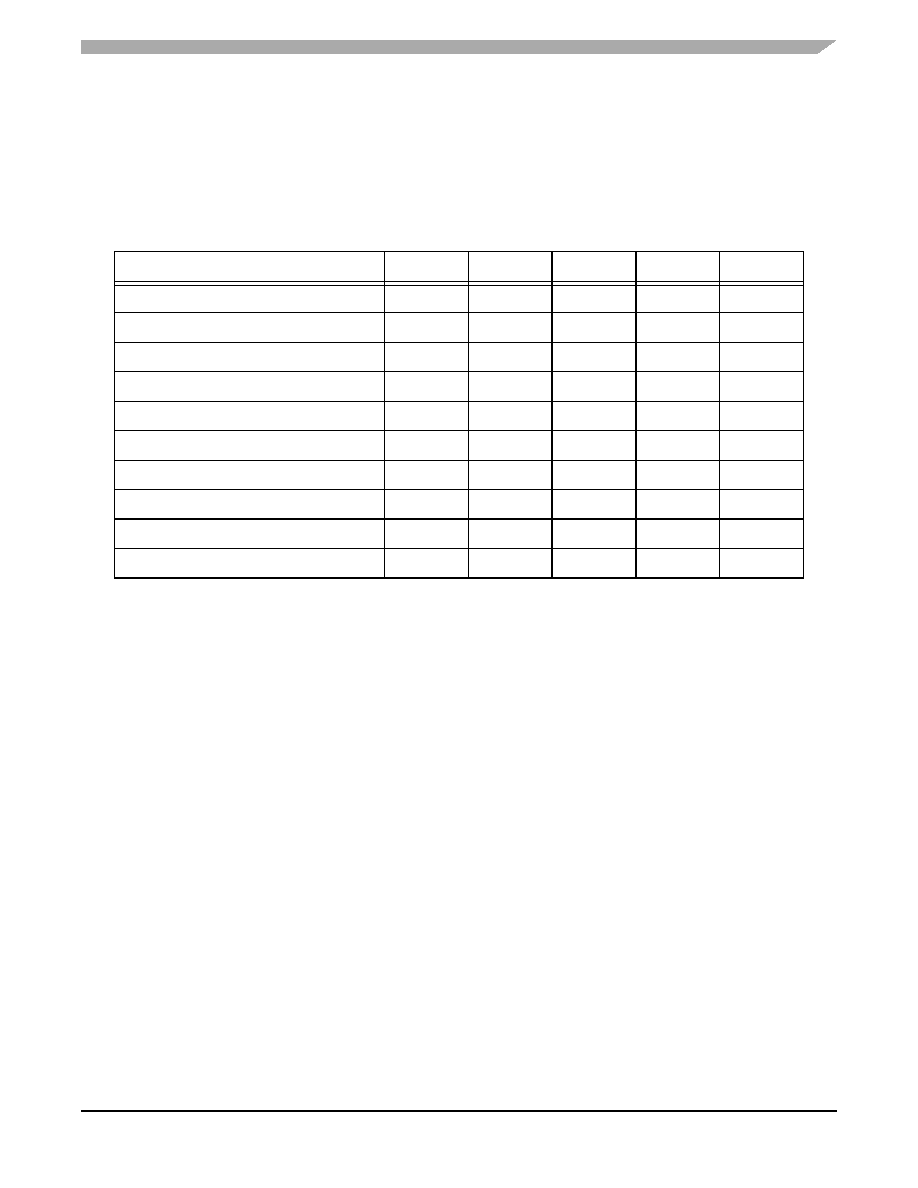
Table 10-15 Crystal Oscillator Parameters
Characteristic
Symbol
Min
Typ
Max
Unit
Crystal Start-up time
TCS
45
10
ms
Resonator Start-up time
TRS
0.1
0.18
1
ms
Crystal ESR
RESR
——
120
ohms
Crystal Peak-to-Peak Jitter
TD
70
—
250
ps
Crystal Min-Max Period Variation
TPV
0.12
—
1.5
ns
Resonator Peak-to-Peak Jitter
TRJ
——
300
ps
Resonator Min-Max Period Variation
TRP
——
300
ps
Bias Current, high-drive mode
IBIASH
—250
290
μA
Bias Current, low-drive mode
IBIASL
—80
110
μA
Quiescent Current, power-down mode
IPD
—0
1
μA
t
= Parameter delay time
D
= Fixed portion of the delay, due to on-chip path delays
P
= Period of the system clock, which determines the execution rate of the part
(i.e., when the device is operating at 60MHz, P = 16.67 ns)
M
= Fixed portion of a clock period inherent in the design; this number is adjusted to account
for possible derating of clock duty cycle
W
= Sum of the applicable wait state controls. The “Wait State Controls” column of
Table 10-16 shows the applicable controls for each parameter and the EMI chapter of the
56F8300 Peripheral User Manual details what each wait state field controls.
相关PDF资料 |
PDF描述 |
|---|---|
| MC68020RP25 | 32-BIT, 25 MHz, MICROPROCESSOR, PPGA114 |
| MC9328MX1DVH20 | 200 MHz, RISC PROCESSOR, PBGA256 |
| MC68HC705J1AVDW | 8-BIT, OTPROM, 2.1 MHz, MICROCONTROLLER, PDSO20 |
| MC68HC908EY16MFA | 8-BIT, FLASH, 8 MHz, MICROCONTROLLER, PQFP32 |
| MC68HSR705J1AP | 8-BIT, OTPROM, MICROCONTROLLER, PDIP20 |
相关代理商/技术参数 |
参数描述 |
|---|---|
| MC56F8346MFVE | 功能描述:数字信号处理器和控制器 - DSP, DSC 16 BIT HYBRID CONTROLLER RoHS:否 制造商:Microchip Technology 核心:dsPIC 数据总线宽度:16 bit 程序存储器大小:16 KB 数据 RAM 大小:2 KB 最大时钟频率:40 MHz 可编程输入/输出端数量:35 定时器数量:3 设备每秒兆指令数:50 MIPs 工作电源电压:3.3 V 最大工作温度:+ 85 C 封装 / 箱体:TQFP-44 安装风格:SMD/SMT |
| MC56F8346VFV60 | 功能描述:数字信号处理器和控制器 - DSP, DSC 60MHz 60MIPS RoHS:否 制造商:Microchip Technology 核心:dsPIC 数据总线宽度:16 bit 程序存储器大小:16 KB 数据 RAM 大小:2 KB 最大时钟频率:40 MHz 可编程输入/输出端数量:35 定时器数量:3 设备每秒兆指令数:50 MIPs 工作电源电压:3.3 V 最大工作温度:+ 85 C 封装 / 箱体:TQFP-44 安装风格:SMD/SMT |
| MC56F8346VFVE | 功能描述:数字信号处理器和控制器 - DSP, DSC 16 BIT HYBRID CNTRLR RoHS:否 制造商:Microchip Technology 核心:dsPIC 数据总线宽度:16 bit 程序存储器大小:16 KB 数据 RAM 大小:2 KB 最大时钟频率:40 MHz 可编程输入/输出端数量:35 定时器数量:3 设备每秒兆指令数:50 MIPs 工作电源电压:3.3 V 最大工作温度:+ 85 C 封装 / 箱体:TQFP-44 安装风格:SMD/SMT |
| MC56F8346VFVER2 | 功能描述:数字信号处理器和控制器 - DSP, DSC 16 BIT HYBRID CNTRLR RoHS:否 制造商:Microchip Technology 核心:dsPIC 数据总线宽度:16 bit 程序存储器大小:16 KB 数据 RAM 大小:2 KB 最大时钟频率:40 MHz 可编程输入/输出端数量:35 定时器数量:3 设备每秒兆指令数:50 MIPs 工作电源电压:3.3 V 最大工作温度:+ 85 C 封装 / 箱体:TQFP-44 安装风格:SMD/SMT |
| MC56F8347 | 制造商:FREESCALE 制造商全称:Freescale Semiconductor, Inc 功能描述:16-bit Digital Signal Controllers |
发布紧急采购,3分钟左右您将得到回复。