- 您现在的位置:买卖IC网 > PDF目录80565 > MC56F8346MFV60 (FREESCALE SEMICONDUCTOR INC) 16-BIT, 120 MHz, OTHER DSP, PQFP144 PDF资料下载
参数资料
| 型号: | MC56F8346MFV60 |
| 厂商: | FREESCALE SEMICONDUCTOR INC |
| 元件分类: | 数字信号处理 |
| 英文描述: | 16-BIT, 120 MHz, OTHER DSP, PQFP144 |
| 封装: | LQFP-144 |
| 文件页数: | 119/178页 |
| 文件大小: | 880K |
| 代理商: | MC56F8346MFV60 |
第1页第2页第3页第4页第5页第6页第7页第8页第9页第10页第11页第12页第13页第14页第15页第16页第17页第18页第19页第20页第21页第22页第23页第24页第25页第26页第27页第28页第29页第30页第31页第32页第33页第34页第35页第36页第37页第38页第39页第40页第41页第42页第43页第44页第45页第46页第47页第48页第49页第50页第51页第52页第53页第54页第55页第56页第57页第58页第59页第60页第61页第62页第63页第64页第65页第66页第67页第68页第69页第70页第71页第72页第73页第74页第75页第76页第77页第78页第79页第80页第81页第82页第83页第84页第85页第86页第87页第88页第89页第90页第91页第92页第93页第94页第95页第96页第97页第98页第99页第100页第101页第102页第103页第104页第105页第106页第107页第108页第109页第110页第111页第112页第113页第114页第115页第116页第117页第118页当前第119页第120页第121页第122页第123页第124页第125页第126页第127页第128页第129页第130页第131页第132页第133页第134页第135页第136页第137页第138页第139页第140页第141页第142页第143页第144页第145页第146页第147页第148页第149页第150页第151页第152页第153页第154页第155页第156页第157页第158页第159页第160页第161页第162页第163页第164页第165页第166页第167页第168页第169页第170页第171页第172页第173页第174页第175页第176页第177页第178页
Interrupt Vector Table
56F8346 Technical Data, Rev. 15
Freescale Semiconductor
45
Preliminary
in the 56F8346/56F8146).
The EMI_MODE pin also affects the reset vector address, as provided in Table 4-4. Additional pins must
be configured as address or chip select signals to access addresses at P:$10 0000 and above.
Note: Program RAM is NOT available on the 56F8146 device.
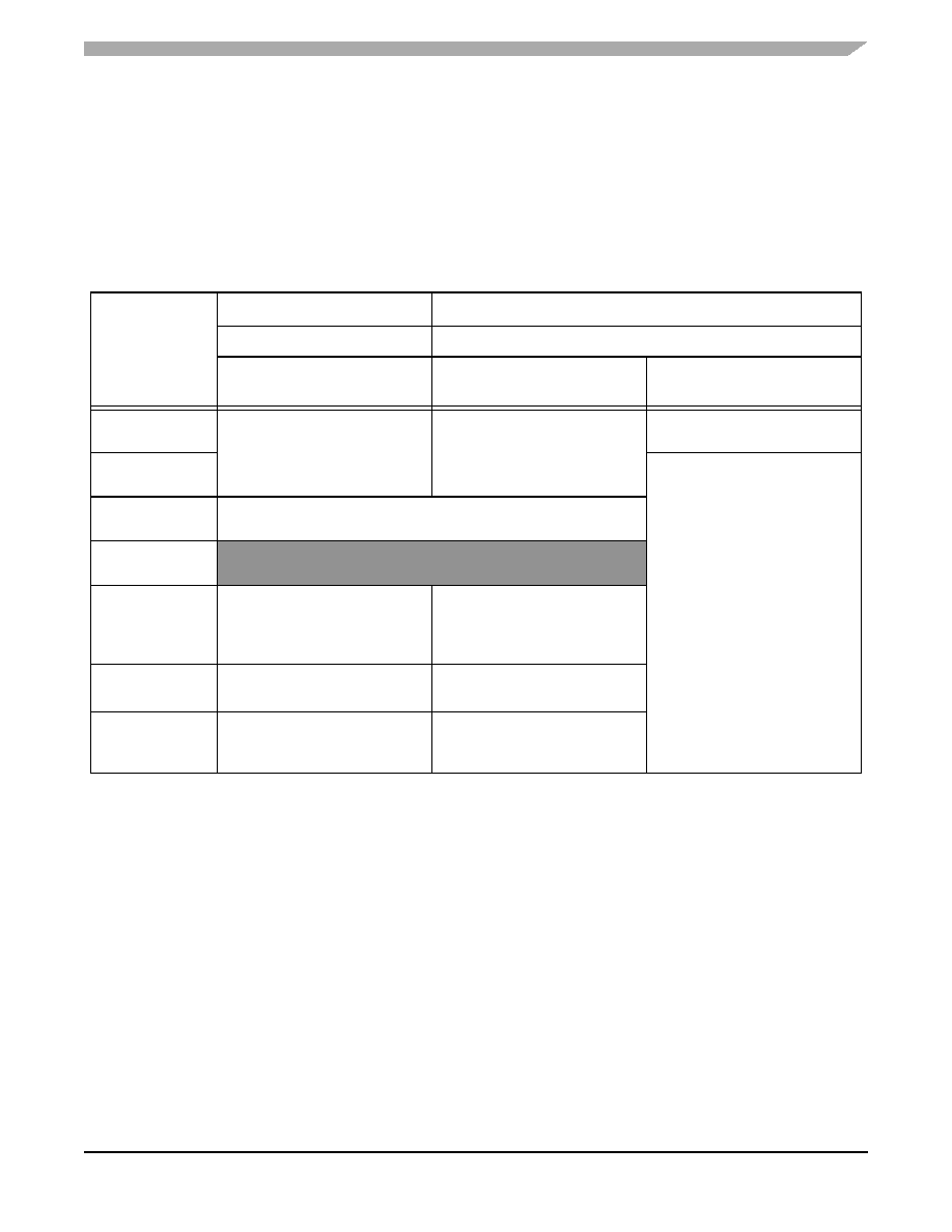
4.3 Interrupt Vector Table
Table 4-5 provides the reset and interrupt priority structure, including on-chip peripherals. The table is
organized with higher-priority vectors at the top and lower-priority interrupts lower in the table. The
priority of an interrupt can be assigned to different levels, as indicated, allowing some control over
Table 4-4 Program Memory Map at Reset
Begin/End
Address
Mode 0 (MA = 0)
Mode 11 (MA = 1)
1. If Flash Security Mode is enabled, EXTBOOT Mode 1 cannot be used. See Security Features, Part 7.
Internal Boot
External Boot
Internal Boot
16-Bit External Address Bus
EMI_MODE = 02,3
16-Bit External Address Bus
2. This mode provides maximum compatibility with 56F80x parts while operating externally.
3. “EMI_MODE =0” when EMI_MODE pin is tied to ground at boot up.
EMI_MODE = 14
20-Bit External Address Bus
4. “EMI_MODE =1” when EMI_MODE pin is tied to VDD at boot up.
P:$1F FFFF
P:$10 0000
External Program Memory5
5. Not accessible in reset configuration, since the address is above P:$00 FFFF. The higher bit address/GPIO (and/or chip se-
lects) pins must be reconfigured before this external memory is accessible.
External Program Memory5
P:$0F FFFF
P:$03 0000
External Program RAM
COP Reset Address = 02 00026
Boot Location = 02 00006
6. Booting from this external address allows prototyping of the internal Boot Flash.
P:$02 FFFF
P:$02 F800
On-Chip Program RAM
4KB
P:$02 F7FF
P:$02 1000
Reserved
116KB
P:$02 0FFF
P:$02 0000
Boot Flash
8KB
COP Reset Address = 02 0002
Boot Location = 02 0000
Boot Flash
8KB
(Not Used for Boot in this Mode)
P:$01 FFFF
P:$01 0000
External Program RAM5
Internal Program Flash7
128KB
7. The internal Program Flash is relocated in this mode making it accessible.
P:$00 FFFF
P:$00 0000
Internal Program Flash
128KB
External Program RAM
COP Reset Address = 00 0002
Boot Location = 00 0000
相关PDF资料 |
PDF描述 |
|---|---|
| MC68020RP25 | 32-BIT, 25 MHz, MICROPROCESSOR, PPGA114 |
| MC9328MX1DVH20 | 200 MHz, RISC PROCESSOR, PBGA256 |
| MC68HC705J1AVDW | 8-BIT, OTPROM, 2.1 MHz, MICROCONTROLLER, PDSO20 |
| MC68HC908EY16MFA | 8-BIT, FLASH, 8 MHz, MICROCONTROLLER, PQFP32 |
| MC68HSR705J1AP | 8-BIT, OTPROM, MICROCONTROLLER, PDIP20 |
相关代理商/技术参数 |
参数描述 |
|---|---|
| MC56F8346MFVE | 功能描述:数字信号处理器和控制器 - DSP, DSC 16 BIT HYBRID CONTROLLER RoHS:否 制造商:Microchip Technology 核心:dsPIC 数据总线宽度:16 bit 程序存储器大小:16 KB 数据 RAM 大小:2 KB 最大时钟频率:40 MHz 可编程输入/输出端数量:35 定时器数量:3 设备每秒兆指令数:50 MIPs 工作电源电压:3.3 V 最大工作温度:+ 85 C 封装 / 箱体:TQFP-44 安装风格:SMD/SMT |
| MC56F8346VFV60 | 功能描述:数字信号处理器和控制器 - DSP, DSC 60MHz 60MIPS RoHS:否 制造商:Microchip Technology 核心:dsPIC 数据总线宽度:16 bit 程序存储器大小:16 KB 数据 RAM 大小:2 KB 最大时钟频率:40 MHz 可编程输入/输出端数量:35 定时器数量:3 设备每秒兆指令数:50 MIPs 工作电源电压:3.3 V 最大工作温度:+ 85 C 封装 / 箱体:TQFP-44 安装风格:SMD/SMT |
| MC56F8346VFVE | 功能描述:数字信号处理器和控制器 - DSP, DSC 16 BIT HYBRID CNTRLR RoHS:否 制造商:Microchip Technology 核心:dsPIC 数据总线宽度:16 bit 程序存储器大小:16 KB 数据 RAM 大小:2 KB 最大时钟频率:40 MHz 可编程输入/输出端数量:35 定时器数量:3 设备每秒兆指令数:50 MIPs 工作电源电压:3.3 V 最大工作温度:+ 85 C 封装 / 箱体:TQFP-44 安装风格:SMD/SMT |
| MC56F8346VFVER2 | 功能描述:数字信号处理器和控制器 - DSP, DSC 16 BIT HYBRID CNTRLR RoHS:否 制造商:Microchip Technology 核心:dsPIC 数据总线宽度:16 bit 程序存储器大小:16 KB 数据 RAM 大小:2 KB 最大时钟频率:40 MHz 可编程输入/输出端数量:35 定时器数量:3 设备每秒兆指令数:50 MIPs 工作电源电压:3.3 V 最大工作温度:+ 85 C 封装 / 箱体:TQFP-44 安装风格:SMD/SMT |
| MC56F8347 | 制造商:FREESCALE 制造商全称:Freescale Semiconductor, Inc 功能描述:16-bit Digital Signal Controllers |
发布紧急采购,3分钟左右您将得到回复。