- 您现在的位置:买卖IC网 > PDF目录80565 > MC56F8346MFV60 (FREESCALE SEMICONDUCTOR INC) 16-BIT, 120 MHz, OTHER DSP, PQFP144 PDF资料下载
参数资料
| 型号: | MC56F8346MFV60 |
| 厂商: | FREESCALE SEMICONDUCTOR INC |
| 元件分类: | 数字信号处理 |
| 英文描述: | 16-BIT, 120 MHz, OTHER DSP, PQFP144 |
| 封装: | LQFP-144 |
| 文件页数: | 93/178页 |
| 文件大小: | 880K |
| 代理商: | MC56F8346MFV60 |
第1页第2页第3页第4页第5页第6页第7页第8页第9页第10页第11页第12页第13页第14页第15页第16页第17页第18页第19页第20页第21页第22页第23页第24页第25页第26页第27页第28页第29页第30页第31页第32页第33页第34页第35页第36页第37页第38页第39页第40页第41页第42页第43页第44页第45页第46页第47页第48页第49页第50页第51页第52页第53页第54页第55页第56页第57页第58页第59页第60页第61页第62页第63页第64页第65页第66页第67页第68页第69页第70页第71页第72页第73页第74页第75页第76页第77页第78页第79页第80页第81页第82页第83页第84页第85页第86页第87页第88页第89页第90页第91页第92页当前第93页第94页第95页第96页第97页第98页第99页第100页第101页第102页第103页第104页第105页第106页第107页第108页第109页第110页第111页第112页第113页第114页第115页第116页第117页第118页第119页第120页第121页第122页第123页第124页第125页第126页第127页第128页第129页第130页第131页第132页第133页第134页第135页第136页第137页第138页第139页第140页第141页第142页第143页第144页第145页第146页第147页第148页第149页第150页第151页第152页第153页第154页第155页第156页第157页第158页第159页第160页第161页第162页第163页第164页第165页第166页第167页第168页第169页第170页第171页第172页第173页第174页第175页第176页第177页第178页
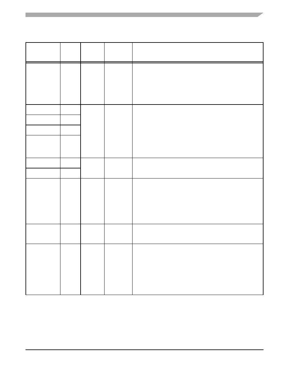
Signal Pins
56F8346 Technical Data, Rev. 15
Freescale Semiconductor
21
Preliminary
OCR_DIS
79
Input
On-Chip Regulator Disable —
Tie this pin to VSS to enable the on-chip regulator
Tie this pin to VDD to disable the on-chip regulator
This pin is intended to be a static DC signal from power-up to
shut down. Do not try to toggle this pin for power savings
during operation.
VCAP1
51
Supply
VCAP1 - 4 — When OCR_DIS is tied to VSS (regulator enabled),
connect each pin to a 2.2
μF or greater bypass capacitor in order to
bypass the core logic voltage regulator, required for proper chip
operation. When OCR_DIS is tied to VDD (regulator disabled),
these pins become VDD_CORE and should be connected to a
regulated 2.5V power supply.
Note: This bypass is required even if the chip is powered with
an external supply.
VCAP2
128
VCAP3
83
VCAP4
15
VPP1
125
Input
VPP1 - 2 — These pins should be left unconnected as an open
circuit for normal functionality.
VPP2
2
CLKMODE
87
Input
Clock Input Mode Selection — This input determines the function
of the XTAL and EXTAL pins.
1 = External clock input on XTAL is used to directly drive the input
clock of the chip. The EXTAL pin should be grounded.
0 = A crystal or ceramic resonator should be connected between
XTAL and EXTAL.
EXTAL
82
Input
External Crystal Oscillator Input — This input can be connected
to an 8MHz external crystal. Tie this pin low if XTAL is driven by an
external clock source.
XTAL
81
Input/
Output
Chip-driven
Crystal Oscillator Output — This output connects the internal
crystal oscillator output to an external crystal.
If an external clock is used, XTAL must be used as the input and
EXTAL connected to GND.
The input clock can be selected to provide the clock directly to the
core. This input clock can also be selected as the input clock for
the on-chip PLL.
Table 2-2 Signal and Package Information for the 144 Pin LQFP
Signal Name
Pin No.
Type
State
During
Reset
Signal Description
相关PDF资料 |
PDF描述 |
|---|---|
| MC68020RP25 | 32-BIT, 25 MHz, MICROPROCESSOR, PPGA114 |
| MC9328MX1DVH20 | 200 MHz, RISC PROCESSOR, PBGA256 |
| MC68HC705J1AVDW | 8-BIT, OTPROM, 2.1 MHz, MICROCONTROLLER, PDSO20 |
| MC68HC908EY16MFA | 8-BIT, FLASH, 8 MHz, MICROCONTROLLER, PQFP32 |
| MC68HSR705J1AP | 8-BIT, OTPROM, MICROCONTROLLER, PDIP20 |
相关代理商/技术参数 |
参数描述 |
|---|---|
| MC56F8346MFVE | 功能描述:数字信号处理器和控制器 - DSP, DSC 16 BIT HYBRID CONTROLLER RoHS:否 制造商:Microchip Technology 核心:dsPIC 数据总线宽度:16 bit 程序存储器大小:16 KB 数据 RAM 大小:2 KB 最大时钟频率:40 MHz 可编程输入/输出端数量:35 定时器数量:3 设备每秒兆指令数:50 MIPs 工作电源电压:3.3 V 最大工作温度:+ 85 C 封装 / 箱体:TQFP-44 安装风格:SMD/SMT |
| MC56F8346VFV60 | 功能描述:数字信号处理器和控制器 - DSP, DSC 60MHz 60MIPS RoHS:否 制造商:Microchip Technology 核心:dsPIC 数据总线宽度:16 bit 程序存储器大小:16 KB 数据 RAM 大小:2 KB 最大时钟频率:40 MHz 可编程输入/输出端数量:35 定时器数量:3 设备每秒兆指令数:50 MIPs 工作电源电压:3.3 V 最大工作温度:+ 85 C 封装 / 箱体:TQFP-44 安装风格:SMD/SMT |
| MC56F8346VFVE | 功能描述:数字信号处理器和控制器 - DSP, DSC 16 BIT HYBRID CNTRLR RoHS:否 制造商:Microchip Technology 核心:dsPIC 数据总线宽度:16 bit 程序存储器大小:16 KB 数据 RAM 大小:2 KB 最大时钟频率:40 MHz 可编程输入/输出端数量:35 定时器数量:3 设备每秒兆指令数:50 MIPs 工作电源电压:3.3 V 最大工作温度:+ 85 C 封装 / 箱体:TQFP-44 安装风格:SMD/SMT |
| MC56F8346VFVER2 | 功能描述:数字信号处理器和控制器 - DSP, DSC 16 BIT HYBRID CNTRLR RoHS:否 制造商:Microchip Technology 核心:dsPIC 数据总线宽度:16 bit 程序存储器大小:16 KB 数据 RAM 大小:2 KB 最大时钟频率:40 MHz 可编程输入/输出端数量:35 定时器数量:3 设备每秒兆指令数:50 MIPs 工作电源电压:3.3 V 最大工作温度:+ 85 C 封装 / 箱体:TQFP-44 安装风格:SMD/SMT |
| MC56F8347 | 制造商:FREESCALE 制造商全称:Freescale Semiconductor, Inc 功能描述:16-bit Digital Signal Controllers |
发布紧急采购,3分钟左右您将得到回复。