- 您现在的位置:买卖IC网 > PDF目录80446 > MC68L11D0FNE2 (FREESCALE SEMICONDUCTOR INC) 8-BIT, 2 MHz, MICROCONTROLLER, PQCC44 PDF资料下载
参数资料
| 型号: | MC68L11D0FNE2 |
| 厂商: | FREESCALE SEMICONDUCTOR INC |
| 元件分类: | 微控制器/微处理器 |
| 英文描述: | 8-BIT, 2 MHz, MICROCONTROLLER, PQCC44 |
| 封装: | PLASTIC, LCC-44 |
| 文件页数: | 127/138页 |
| 文件大小: | 1047K |
| 代理商: | MC68L11D0FNE2 |
第1页第2页第3页第4页第5页第6页第7页第8页第9页第10页第11页第12页第13页第14页第15页第16页第17页第18页第19页第20页第21页第22页第23页第24页第25页第26页第27页第28页第29页第30页第31页第32页第33页第34页第35页第36页第37页第38页第39页第40页第41页第42页第43页第44页第45页第46页第47页第48页第49页第50页第51页第52页第53页第54页第55页第56页第57页第58页第59页第60页第61页第62页第63页第64页第65页第66页第67页第68页第69页第70页第71页第72页第73页第74页第75页第76页第77页第78页第79页第80页第81页第82页第83页第84页第85页第86页第87页第88页第89页第90页第91页第92页第93页第94页第95页第96页第97页第98页第99页第100页第101页第102页第103页第104页第105页第106页第107页第108页第109页第110页第111页第112页第113页第114页第115页第116页第117页第118页第119页第120页第121页第122页第123页第124页第125页第126页当前第127页第128页第129页第130页第131页第132页第133页第134页第135页第136页第137页第138页
Input Capture
MC68HC711D3 Data Sheet, Rev. 2.1
Freescale Semiconductor
89
8.3.1 Timer Control 2 Register
Use the control bits of timer control 2 register (TCTL2) to program input capture functions to detect a
particular edge polarity on the corresponding timer input pin. Each of the input capture functions can be
independently configured to detect rising edges only, falling edges only, any edge (rising or falling), or to
disable the input capture function. The input capture functions operate independently of each other and
can capture the same TCNT value if the input edges are detected within the same timer count cycle.
EDGxB and EDGxA — Input Capture Edge Control
There are four pairs of these bits. Each pair is cleared to 0 by reset and must be encoded to configure
the corresponding input capture edge detector circuit. IC4 functions only if the I4/O5 bit in PACTL is
set. Refer to Table 8-2 for timer control configuration.
8.3.2 Timer Input Capture Registers
When an edge has been detected and synchronized, the 16-bit free-running counter value is transferred
into the input capture register pair as a single 16-bit parallel transfer. Timer counter value captures and
timer counter incrementing occur on opposite half-cycles of the phase two clock so that the count value
is stable whenever a capture occurs. The timer input capture (TICx) registers are not affected by reset.
Input capture values can be read from a pair of 8-bit read-only registers. A read of the high-order byte of
an input capture register pair inhibits a new capture transfer for one bus cycle. If a double-byte read
instruction, such as LDD, is used to read the captured value, coherency is assured. When a new input
capture occurs immediately after a high-order byte read, transfer is delayed for an additional cycle but the
value is not lost.
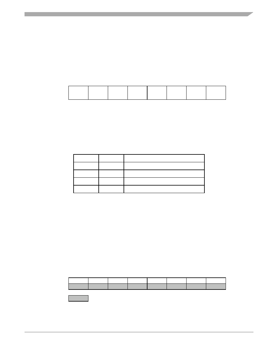
Address:
$0021
Bit 7
654321
Bit 0
Read:
EDG4B
EDG4A
EDG1B
EDG1A
EDG2B
EDG2A
EDG3B
EDG3A
Write:
Reset:
00000000
Figure 8-3. Timer Control 2 Register (TCTL2)
Table 8-2. Timer Control Configuration
EDGxB
EDGxA
Configuration
0
Capture disabled
0
1
Capture on rising edges only
1
0
Capture on falling edges only
1
Capture on any edge
Address: $0010 — TIC1 (High)
Bit 15
14
13
12
11
10
9
Bit 8
Read:
Bit 15
Bit 14
Bit 13
Bit 12
Bit 11
Bit 10
Bit 9
Bit 8
Write:
Reset:
Unaffected by reset
= Unimplemented
Figure 8-4. Timer Input Capture Registers (TICx)
相关PDF资料 |
PDF描述 |
|---|---|
| MC908GR60AVFAR2 | 8-BIT, FLASH, 8 MHz, MICROCONTROLLER, PQFP48 |
| MC908GZ48VFAE | 8-BIT, FLASH, 8 MHz, MICROCONTROLLER, PQFP48 |
| MC908GZ60CFJE | 8-BIT, FLASH, 8 MHz, MICROCONTROLLER, PQFP32 |
| MC9S08RE16FGE | 8-BIT, FLASH, 8 MHz, MICROCONTROLLER, PQFP44 |
| MC9S12C96CPBR2 | 16-BIT, FLASH, 25 MHz, MICROCONTROLLER, PQFP52 |
相关代理商/技术参数 |
参数描述 |
|---|---|
| MC68L11E0FN2 | 制造商:Rochester Electronics LLC 功能描述:8-BIT MCU,512RAM,A/D,LVDC - Bulk |
| MC68L11E0FNE2 | 功能描述:IC MCU 8BIT LV 512RAM 52-PLCC RoHS:是 类别:集成电路 (IC) >> 嵌入式 - 微控制器, 系列:HC11 标准包装:1 系列:87C 核心处理器:MCS 51 芯体尺寸:8-位 速度:16MHz 连通性:SIO 外围设备:- 输入/输出数:32 程序存储器容量:8KB(8K x 8) 程序存储器类型:OTP EEPROM 大小:- RAM 容量:256 x 8 电压 - 电源 (Vcc/Vdd):4 V ~ 6 V 数据转换器:- 振荡器型:外部 工作温度:0°C ~ 70°C 封装/外壳:44-DIP 包装:管件 其它名称:864285 |
| MC68L11E1CFNE2 | 功能描述:8位微控制器 -MCU 8B MCU RAM EE A/D LVDC RoHS:否 制造商:Silicon Labs 核心:8051 处理器系列:C8051F39x 数据总线宽度:8 bit 最大时钟频率:50 MHz 程序存储器大小:16 KB 数据 RAM 大小:1 KB 片上 ADC:Yes 工作电源电压:1.8 V to 3.6 V 工作温度范围:- 40 C to + 105 C 封装 / 箱体:QFN-20 安装风格:SMD/SMT |
| MC68L11E1FNE2 | 功能描述:8位微控制器 -MCU 8B MCU RAM EE A/D LVD RoHS:否 制造商:Silicon Labs 核心:8051 处理器系列:C8051F39x 数据总线宽度:8 bit 最大时钟频率:50 MHz 程序存储器大小:16 KB 数据 RAM 大小:1 KB 片上 ADC:Yes 工作电源电压:1.8 V to 3.6 V 工作温度范围:- 40 C to + 105 C 封装 / 箱体:QFN-20 安装风格:SMD/SMT |
| MC68L11F1CFNE3 | 功能描述:8位微控制器 -MCU 8B MCU 1KRAM 512BYTES RoHS:否 制造商:Silicon Labs 核心:8051 处理器系列:C8051F39x 数据总线宽度:8 bit 最大时钟频率:50 MHz 程序存储器大小:16 KB 数据 RAM 大小:1 KB 片上 ADC:Yes 工作电源电压:1.8 V to 3.6 V 工作温度范围:- 40 C to + 105 C 封装 / 箱体:QFN-20 安装风格:SMD/SMT |
发布紧急采购,3分钟左右您将得到回复。