- 您现在的位置:买卖IC网 > PDF目录11944 > MC705C9ACPE (Freescale Semiconductor)IC MCU 2.1MHZ 16K OTP 40-DIP PDF资料下载
参数资料
| 型号: | MC705C9ACPE |
| 厂商: | Freescale Semiconductor |
| 文件页数: | 78/118页 |
| 文件大小: | 0K |
| 描述: | IC MCU 2.1MHZ 16K OTP 40-DIP |
| 标准包装: | 9 |
| 系列: | HC05 |
| 核心处理器: | HC05 |
| 芯体尺寸: | 8-位 |
| 速度: | 2.1MHz |
| 连通性: | SCI,SPI |
| 外围设备: | POR,WDT |
| 输入/输出数: | 24 |
| 程序存储器容量: | 16KB(16K x 8) |
| 程序存储器类型: | OTP |
| RAM 容量: | 352 x 8 |
| 电压 - 电源 (Vcc/Vdd): | 3 V ~ 5.5 V |
| 振荡器型: | 内部 |
| 工作温度: | -40°C ~ 85°C |
| 封装/外壳: | 40-DIP(0.600",15.24mm) |
| 包装: | 管件 |
第1页第2页第3页第4页第5页第6页第7页第8页第9页第10页第11页第12页第13页第14页第15页第16页第17页第18页第19页第20页第21页第22页第23页第24页第25页第26页第27页第28页第29页第30页第31页第32页第33页第34页第35页第36页第37页第38页第39页第40页第41页第42页第43页第44页第45页第46页第47页第48页第49页第50页第51页第52页第53页第54页第55页第56页第57页第58页第59页第60页第61页第62页第63页第64页第65页第66页第67页第68页第69页第70页第71页第72页第73页第74页第75页第76页第77页当前第78页第79页第80页第81页第82页第83页第84页第85页第86页第87页第88页第89页第90页第91页第92页第93页第94页第95页第96页第97页第98页第99页第100页第101页第102页第103页第104页第105页第106页第107页第108页第109页第110页第111页第112页第113页第114页第115页第116页第117页第118页
Serial Communications Interface (SCI)
MC68HC05C9A Advance Information Data Sheet, Rev. 4.1
62
Freescale Semiconductor
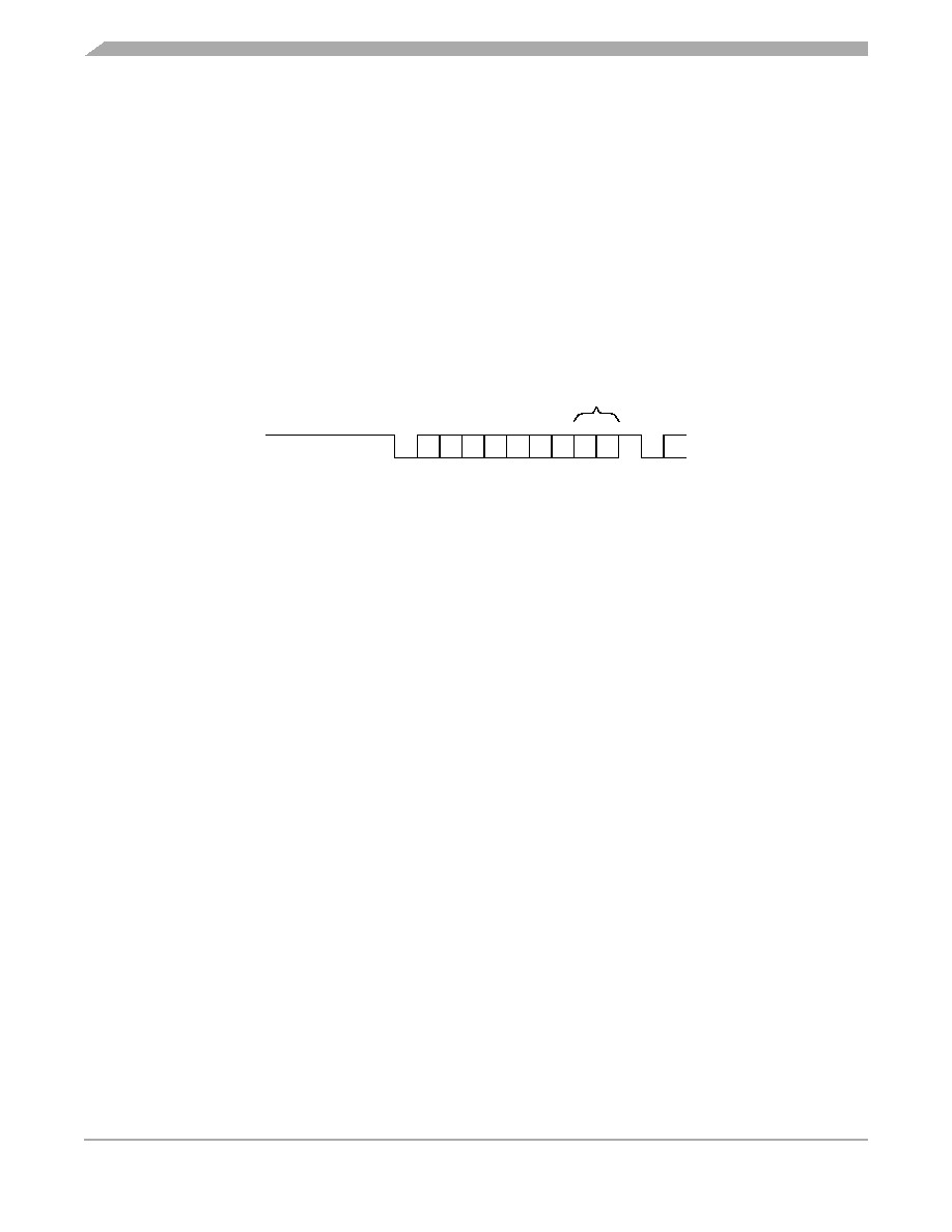
9.6 Data Format
Receive data or transmit data is the serial data that is transferred to the internal data bus from the receive
data input pin (RDI) or from the internal bus to the transmit data output pin (TDO). The non-return-to-zero
(NRZ) data format shown in Figure 9-3 is used and must meet the following criteria:
The idle line is brought to a logic 1 state prior to transmission/reception of a character.
A start bit (logic 0) is used to indicate the start of a frame.
The data is transmitted and received least significant bit first.
A stop bit (logic 1) is used to indicate the end of a frame. A frame consists of a start bit, a character
of eight or nine data bits, and a stop bit.
A break is defined as the transmission or reception of a low (logic 0) for at least one complete frame
time.
Figure 9-3. Data Format
9.7 Receiver Wakeup Operation
The receiver logic hardware also supports a receiver wakeup function which is intended for systems
having more than one receiver. With this function a transmitting device directs messages to an individual
receiver or group of receivers by passing addressing information as the initial byte(s) of each message.
The wakeup function allows receivers not addressed to remain in a dormant state for the remainder of the
unwanted message. This eliminates any further software overhead to service the remaining characters of
the unwanted message and thus improves system performance.
The receiver is placed in wakeup mode by setting the receiver wakeup bit (RWU) in the SCCR2 register.
While RWU is set, all of the receiver-related status flags (RDRF, IDLE, OR, NF, and FE) are inhibited
(cannot become set).
NOTE
The idle line detect function is inhibited while the RWU bit is set. Although
RWU may be cleared by a software write to SCCR2, it would be unusual to
do so.
Normally, RWU is set by software and is cleared automatically in hardware by one of these methods: idle
line wakeup or address mark wakeup.
9.8 Idle Line Wakeup
In idle line wakeup mode, a dormant receiver wakes up as soon as the RDI line becomes idle. Idle is
defined as a continuous logic high level on the RDI line for 10 (or 11) full bit times. Systems using this
type of wakeup must provide at least one character time of idle between messages to wake up sleeping
receivers, but must not allow any idle time between characters within a message.
IDLE LINE
012345678
0
STOP START
START
CONTROL BIT M SELECTS
8- OR 9-BIT DATA
相关PDF资料 |
PDF描述 |
|---|---|
| 2-6457567-2 | ADPTR,DUP,LC,SR BLU,CER,LOGO |
| V24A28T400BF3 | CONVERTER MOD DC/DC 28V 400W |
| V24A28T400BF2 | CONVERTER MOD DC/DC 28V 400W |
| V24A24T400BG3 | CONVERTER MOD DC/DC 24V 400W |
| V24A24T400BG2 | CONVERTER MOD DC/DC 24V 400W |
相关代理商/技术参数 |
参数描述 |
|---|---|
| MC705E6CDWE | 制造商:Freescale Semiconductor 功能描述: |
| MC705J1A | 制造商:Freescale Semiconductor 功能描述: |
| MC705J1ACDWE | 功能描述:8位微控制器 -MCU HCO5 CORE+1.2K RAM + EPR RoHS:否 制造商:Silicon Labs 核心:8051 处理器系列:C8051F39x 数据总线宽度:8 bit 最大时钟频率:50 MHz 程序存储器大小:16 KB 数据 RAM 大小:1 KB 片上 ADC:Yes 工作电源电压:1.8 V to 3.6 V 工作温度范围:- 40 C to + 105 C 封装 / 箱体:QFN-20 安装风格:SMD/SMT |
| MC705J1ACDWE | 制造商:Freescale Semiconductor 功能描述:8-Bit Microcontroller IC |
| MC705JJ7CDWE | 功能描述:8位微控制器 -MCU 705JJ7 224 BYTES RAM RoHS:否 制造商:Silicon Labs 核心:8051 处理器系列:C8051F39x 数据总线宽度:8 bit 最大时钟频率:50 MHz 程序存储器大小:16 KB 数据 RAM 大小:1 KB 片上 ADC:Yes 工作电源电压:1.8 V to 3.6 V 工作温度范围:- 40 C to + 105 C 封装 / 箱体:QFN-20 安装风格:SMD/SMT |
发布紧急采购,3分钟左右您将得到回复。