- 您现在的位置:买卖IC网 > PDF目录26811 > MC88921DW (INTEGRATED DEVICE TECHNOLOGY INC) 88921 SERIES, PLL BASED CLOCK DRIVER, 5 TRUE OUTPUT(S), 0 INVERTED OUTPUT(S), PDSO20 PDF资料下载
参数资料
| 型号: | MC88921DW |
| 厂商: | INTEGRATED DEVICE TECHNOLOGY INC |
| 元件分类: | 时钟及定时 |
| 英文描述: | 88921 SERIES, PLL BASED CLOCK DRIVER, 5 TRUE OUTPUT(S), 0 INVERTED OUTPUT(S), PDSO20 |
| 封装: | SOIC-20 |
| 文件页数: | 10/11页 |
| 文件大小: | 544K |
| 代理商: | MC88921DW |
MC88921
MOTOROLA
TIMING SOLUTIONS
BR1333 — REV 5
8
The tPD spec includes the full temperature range from 0°C
to 70
°C and the full VCC range from 4.75V to 5.25V. If the
T and VCC is a given system are less than the
specification limits, the tPD spec window will be reduced.
The tPD window for a given T and VCC is given by the
following regression formula:
TBD
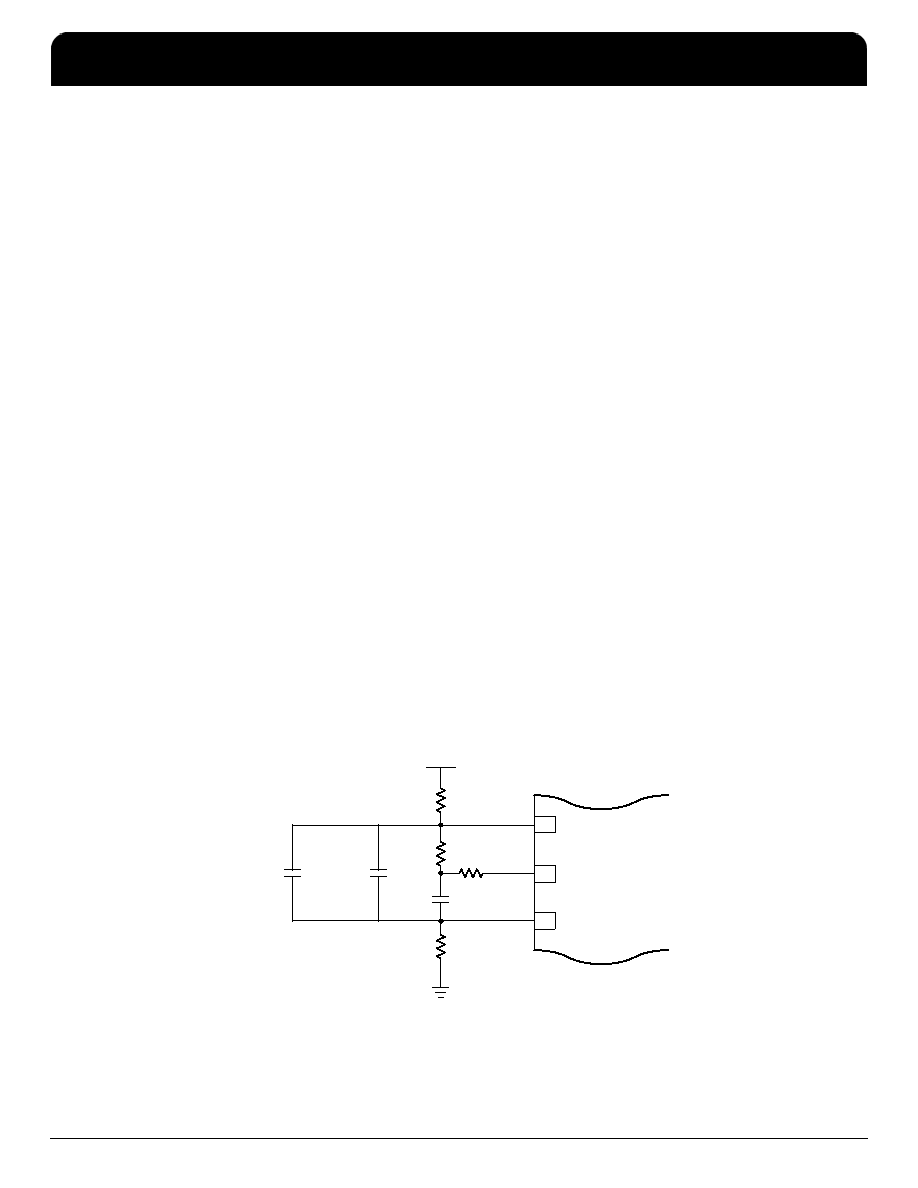
Notes Concerning Loop Filter and Board Layout Issues
1. Figure 7 shows a loop filter and analog isolation scheme
which will be effective in most applications. The following
guidelines should be followed to ensure stable and
jitter–free operation:
1a. All loop filter and analog isolation components should be
tied as close to the package as possible. Stray current
passing through the parasitics of long traces can cause
undesirable voltage transients at the RC1 pin.
1b. The 47
resistors, the 10F low frequency bypass
capacitor, and the 0.1
F high frequency bypass capacitor
form a wide bandwidth filter that will make the 88921 PLL
insensitive to voltage transients from the system digital
VCC supply and ground planes. This filter will typically
ensure that a 100mV step deviation on the digital VCC
supply will cause no more than a 100ps phase deviation
on the 88921 outputs. A 250mV step deviation on VCC
using the recommended filter values will cause no more
than a 250ps phase deviation; if a 25
F bypass capacitor
is used (instead of 10
F) a 250mV VCC step will cause no
more than a 100ps phase deviation.
If good bypass techniques are used on a board design
near components which may cause digital VCC and
ground noise, the above described VCC step deviations
should not occur at the 88921’s digital VCC supply. The
purpose of the bypass filtering scheme shown in Figure 7
is to give the 88921 additional protection from the power
supply and ground plane transients that can occur in a
high frequency, high speed digital system.
1c. There are no special requirements set forth for the loop
filter resistors (1M and 330
). The loop filter capacitor
(0.1uF) can be a ceramic chip capacitor, the same as a
standard bypass capacitor.
1d. The 1M reference resistor injects current into the internal
charge pump of the PLL, causing a fixed offset between
the outputs and the SYNC input. This also prevents
excessive jitter caused by inherent PLL dead–band. If the
VCO (2X_Q output) is running above 40MHz, the 1M
resistor provides the correct amount of current injection
into the charge pump (2–3
A).
2. In addition to the bypass capacitors used in the analog
filter of Figure 7, there should be a 0.1
F bypass
capacitor between each of the other (digital) four VCC
pins and the board ground plane. This will reduce output
switching noise caused by the 88921 outputs, in addition
to reducing potential for noise in the ‘analog’ section of
the chip. These bypass capacitors should also be tied as
close to the 88921 package as possible.
Figure 6. Recommended Loop Filter and Analog Isolation Scheme for the MC88921
47
BOARD VCC
0.1
F (LOOP
FILTER CAP)
330
1M
0.1
F HIGH
FREQ BIAS
10
F LOW
FREQ BIAS
47
BOARD GND
5
6
7
ANALOG VCC
RC1
ANALOG GND
ANALOG LOOP FILTER/VCO
SECTION OF THE MC88921
20–PIN SOIC PACKAGE (NOT
DRAWN TO SCALE)
A SEPARATE ANALOG POWER SUPPLY IS NOT NECESSARY AND
SHOULD NOT BE USED. FOLLOWING THESE PRESCRIBED GUIDE-
LINES IS ALL THAT IS NECESSARY TO USE THE MC88921 IN A NORMAL
DIGITAL ENVIRONMENT.
F
re
e
sc
a
le
S
e
m
ic
o
n
d
u
c
to
r,
I
Freescale Semiconductor, Inc.
For More Information On This Product,
Go to: www.freescale.com
n
c
..
.
MC88921
Low Skew CMOS PLL Clock Drivers With Power-Down/Power-up Feature
NETCOM
IDT Low Skew CMOS PLL Clock Drivers With Power-Down/Power-up Feature
Freescale Timing Solutions Organization has been acquired by Integrated Device Technology, Inc
MC88921
8
相关PDF资料 |
PDF描述 |
|---|---|
| MC88LV915TFN | 88LV SERIES, PLL BASED CLOCK DRIVER, 7 TRUE OUTPUT(S), 1 INVERTED OUTPUT(S), PQCC28 |
| MC88LV926DW | 88LV SERIES, PLL BASED CLOCK DRIVER, 4 TRUE OUTPUT(S), 1 INVERTED OUTPUT(S), PDSO20 |
| MD2FLDL-TTL-35G | ACTIVE DELAY LINE, TRUE OUTPUT, DSO6 |
| MD2FLDL-TTL-7F | ACTIVE DELAY LINE, TRUE OUTPUT, DIP6 |
| MD2FLDL-TTL-80G | ACTIVE DELAY LINE, TRUE OUTPUT, DSO6 |
相关代理商/技术参数 |
参数描述 |
|---|---|
| MC889AL | 制造商:Rochester Electronics LLC 功能描述:- Bulk |
| MC889AP | 制造商:Motorola Inc 功能描述: 制造商:MOTOROLA 功能描述: |
| MC88A | 制造商:未知厂家 制造商全称:未知厂家 功能描述:8 TUNES 8 KEY WITH SCAN KEY |
| MC88B/IVY | 制造商:TELEPHONE EQUIPMENT 功能描述:THREE COUPLER 8P8C |
| MC88I TERMINAL | 制造商:MC TECHNOLOGIES 功能描述:MOD GSM / GPRS QUADBAND TERMI 制造商:MC TECHNOLOGIES 功能描述:MOD, GSM / GPRS QUADBAND TERMINAL 制造商:MC TECHNOLOGIES 功能描述:MOD, GSM / GPRS QUADBAND TERMINAL; No. of Channels:4; Protocol:TCP / IP; Supply Voltage Min:8V; Supply Voltage Max:30V; Frequency RF:1.9GHz; Module Interface:RS232, USB; Kit Features:GPRS upto 86kbps, Data CSD upto 14.4kbps, Secure ;RoHS Compliant: Yes |
发布紧急采购,3分钟左右您将得到回复。