- 您现在的位置:买卖IC网 > PDF目录26811 > MC88921DW (INTEGRATED DEVICE TECHNOLOGY INC) 88921 SERIES, PLL BASED CLOCK DRIVER, 5 TRUE OUTPUT(S), 0 INVERTED OUTPUT(S), PDSO20 PDF资料下载
参数资料
| 型号: | MC88921DW |
| 厂商: | INTEGRATED DEVICE TECHNOLOGY INC |
| 元件分类: | 时钟及定时 |
| 英文描述: | 88921 SERIES, PLL BASED CLOCK DRIVER, 5 TRUE OUTPUT(S), 0 INVERTED OUTPUT(S), PDSO20 |
| 封装: | SOIC-20 |
| 文件页数: | 8/11页 |
| 文件大小: | 544K |
| 代理商: | MC88921DW |
MC88921
MOTOROLA
TIMING SOLUTIONS
BR1333 — REV 5
6
Application Notes
1. Several specifications can only be measured when the
MC88921 is in phase–locked operation. It is not possible
to have the part in phase–lock on ATE (automated test
equipment). Statistical characterization techniques were
used to guarantee those specifications which cannot be
measured on the ATE. MC88921 units were fabricated
with key transistor properties intentionally varied to create
a 14 cell designed experimental matrix. IC performance
was characterized over a range of transistor properties
(represented by the 14 cells) in excess of the expected
process variation of the wafer fabrication area.
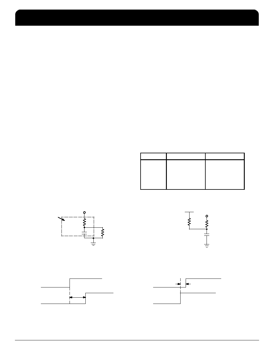
2. A 1M
resistor tied to either Analog VCC or Analog GND,
as shown in Figure 2, is required to ensure no jitter is
present on the MC88921 outputs. This technique causes
a phase offset between the SYNC input and the Q0
output, measured at the pins. The tPD spec describes how
this offset varies with process, temperature, and voltage.
The specs were arrived at by measuring the phase
relationship for the 14 lots described in note 1 while the
part was in phase–locked operation. The actual
measurements were made with a 10MHz SYNC input
(1.0ns edge rate from 0.8V to 2.0V). The phase
measurements were made at 1.5V. See Figure 2 for a
graphical description.
3. Two specs (tRISE/FALL and tPULSE Width 2X_Q output,
see AC Specifications) guarantee that the MC88921
meets the 20MHz, 25MHz and 33MHz 68040 P–Clock
input specification (at 40MHz, 50MHz, and 66MHz). For
these two specs to be guaranteed by Motorola, the
termination scheme shown in Figure 3 must be used. For
applications which require 1.5V thresholds, but do not
require a tight duty cycle the RP resistor can be ignored.
4. The tPD spec (SYNC to Q/2) guarantees how close the
Q/2 output will be locked to the reference input connected
to the SYNC input (including temperature and voltage
variation). This also tells what the skew from the Q/2
output on one part connected to a given reference input, to
the Q/2 output on one or more parts connected to that
reference input (assuming equal delay from the reference
input to the SYNC input of each part). Therefore the tPD
spec is equivalent to a part–to–part specification.
However, to correctly predict the skew from a given output
on one part to any other output on one or more other parts,
the distribution of each output in relation to the SYNC
input must be known. This distribution for the MC88921 is
provided in Table 1.
TABLE 1.
Distribution of Each Output versus SYNC
Output
–(ps)
+(ps)
2X_Q
Q0
Q1
Q2
Q3
Q/2
TBD
Figure 2. Depiction of the Fixed SYNC to Q0 Offset (tPD) Which Is Present
When a 1M
Resistor Is Tied to VCC or Ground
1M
REFERENCE
RESISTOR
EXTERNAL
LOOP FILTER
330
0.1
F
ANALOG GND
RC1
R2
C1
WITH THE 1M
RESISTOR TIED IN THIS FASHION THE TPD
SPECIFICATION, MEASURED AT THE INPUT PINS IS:
SYNC INPUT
Q0 OUTPUT
2.25ns
OFFSET
3V
5V
tPD = 2.25ns ± 1.0ns (TYPICAL VALUES)
SYNC INPUT
Q0 OUTPUT
–0.8ns
OFFSET
3V
5V
1M
REFERENCE
RESISTOR
330
0.1
F
ANALOG GND
ANALOG VCC
R2
C1
WITH THE 1M
RESISTOR TIED IN THIS FASHION THE TPD
SPECIFICATION, MEASURED AT THE INPUT PINS IS:
tPD = –0.80ns ± 0.30ns
RC1
F
re
e
sc
a
le
S
e
m
ic
o
n
d
u
c
to
r,
I
Freescale Semiconductor, Inc.
For More Information On This Product,
Go to: www.freescale.com
n
c
..
.
MC88921
Low Skew CMOS PLL Clock Drivers With Power-Down/Power-up Feature
NETCOM
IDT Low Skew CMOS PLL Clock Drivers With Power-Down/Power-up Feature
Freescale Timing Solutions Organization has been acquired by Integrated Device Technology, Inc
MC88921
6
相关PDF资料 |
PDF描述 |
|---|---|
| MC88LV915TFN | 88LV SERIES, PLL BASED CLOCK DRIVER, 7 TRUE OUTPUT(S), 1 INVERTED OUTPUT(S), PQCC28 |
| MC88LV926DW | 88LV SERIES, PLL BASED CLOCK DRIVER, 4 TRUE OUTPUT(S), 1 INVERTED OUTPUT(S), PDSO20 |
| MD2FLDL-TTL-35G | ACTIVE DELAY LINE, TRUE OUTPUT, DSO6 |
| MD2FLDL-TTL-7F | ACTIVE DELAY LINE, TRUE OUTPUT, DIP6 |
| MD2FLDL-TTL-80G | ACTIVE DELAY LINE, TRUE OUTPUT, DSO6 |
相关代理商/技术参数 |
参数描述 |
|---|---|
| MC889AL | 制造商:Rochester Electronics LLC 功能描述:- Bulk |
| MC889AP | 制造商:Motorola Inc 功能描述: 制造商:MOTOROLA 功能描述: |
| MC88A | 制造商:未知厂家 制造商全称:未知厂家 功能描述:8 TUNES 8 KEY WITH SCAN KEY |
| MC88B/IVY | 制造商:TELEPHONE EQUIPMENT 功能描述:THREE COUPLER 8P8C |
| MC88I TERMINAL | 制造商:MC TECHNOLOGIES 功能描述:MOD GSM / GPRS QUADBAND TERMI 制造商:MC TECHNOLOGIES 功能描述:MOD, GSM / GPRS QUADBAND TERMINAL 制造商:MC TECHNOLOGIES 功能描述:MOD, GSM / GPRS QUADBAND TERMINAL; No. of Channels:4; Protocol:TCP / IP; Supply Voltage Min:8V; Supply Voltage Max:30V; Frequency RF:1.9GHz; Module Interface:RS232, USB; Kit Features:GPRS upto 86kbps, Data CSD upto 14.4kbps, Secure ;RoHS Compliant: Yes |
发布紧急采购,3分钟左右您将得到回复。