- 您现在的位置:买卖IC网 > PDF目录45311 > MCF5275CVM133 (FREESCALE SEMICONDUCTOR INC) 32-BIT, 133 MHz, RISC PROCESSOR, PBGA256 PDF资料下载
参数资料
| 型号: | MCF5275CVM133 |
| 厂商: | FREESCALE SEMICONDUCTOR INC |
| 元件分类: | 微控制器/微处理器 |
| 英文描述: | 32-BIT, 133 MHz, RISC PROCESSOR, PBGA256 |
| 封装: | MAPBGA-256 |
| 文件页数: | 22/44页 |
| 文件大小: | 1242K |
| 代理商: | MCF5275CVM133 |
第1页第2页第3页第4页第5页第6页第7页第8页第9页第10页第11页第12页第13页第14页第15页第16页第17页第18页第19页第20页第21页当前第22页第23页第24页第25页第26页第27页第28页第29页第30页第31页第32页第33页第34页第35页第36页第37页第38页第39页第40页第41页第42页第43页第44页
Preliminary Electrical Characteristics
MCF5275 Integrated Microprocessor Family Hardware Specification, Rev. 2
Preliminary—Subject to Change Without Notice
Freescale Semiconductor
29
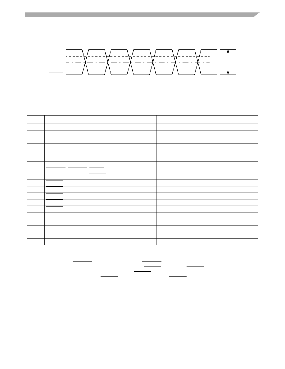
Figure 11. DDR Clock Timing Diagram
When using the DDR SDRAM controller the timing numbers in Table 15 must be followed to properly
latch or drive data onto the memory bus. All timing numbers are relative to the two DQS byte lanes.
Figure 13 shows a DDR SDRAM write cycle.
1
SD VDD is nominally 2.5V.
Table 15. DDR Timing
NUM
Characteristic1
1
All timing specifications are based on taking into account, a 25pF load on the SDRAM output pins.
Symbol
Min
Max
Unit
Frequency of operation2
2
DDR_CLKOUT operates at half the frequency of the PLLMRFM output and the ColdFire core.
TBD
83
MHz
DD1
Clock Period (DDR_CLKOUT)
tCK
12
TBD
ns
DD2
Pulse Width High3
3
tCKH + tCKL must be less than or equal to tCK.
tCKH
0.45
0.55
tCK
DD3
Pulse Width Low3
tCKl
0.45
0.55
tCK
DD4
DDR_CLKOUT high to DDR address, SD_CKE,
SD_CS[1:0], SD_SCAS, SD_SRAS, SD_WE valid
tCMV
—
0.5 x tCK + 1
ns
DD5
DDR_CLKOUT high to DDR address, SD_CKE, SD_CS,
SD_SCAS, SD_SRAS, SD_WE invalid
tCMH
2—
ns
DD6
Write command to first SD_DQS Latching Transition
tDQSS
—1.25
tCK
DD7
SD_DQS high to Data and DM valid (write) - setup4,5
4
D[31:24] is relative to SD_DQS3 and D[23:16] is relative to SD_DQS2.
5
The first data beat will be valid before the first rising edge of SD_DQS and after the SD_DQS write preamble. The
remaining data beats will be valid for each subsequent SD_DQS edge
tQS
1.5
—
ns
DD8
SD_DQS high to Data and DM invalid (write) - hold4
tQH
1—
ns
DD9
SD_DQS high to Data valid (read) - setup6
6
Data input skew is derived from each SD_DQS clock edge. It begins with a SD_DQS transition and ends when the last data
line becomes valid. This input skew must include DDR memory output skew and system level board skew (due to routing or
other factors).
tIS
—1
ns
DD10
SD_DQS high to Data invalid (read) - hold7
7
Data input hold is derived from each SD_DQS clock edge. It begins with a SD_DQS transition and ends when the first data
line becomes invalid.
tIH
0.25 x tCK + 1
—
ns
DD11
SD_DQS falling edge to CLKOUT high - setup
tDSS
0.5
—
ns
DD12
SD_DQS falling edge to CLKOUT high - hold
tDSH
0.5
—
ns
DD13
DQS input read preamble width (tRPRE)tRPRE
0.9
1.1
tCK
DD14
DQS input read postamble width (tRPST)tRPST
0.4
0.6
tCK
DD15
DQS output write preamble width (tWPRE)tWPRE
0.25
—
tCK
DD16
DQS output write postamble width (tWPST)tWPST
0.4
0.6
tCK
SDCLK
VIX
VMP
VIX
VID
相关PDF资料 |
PDF描述 |
|---|---|
| MCF5274VM133 | 32-BIT, 133 MHz, RISC PROCESSOR, PBGA256 |
| MCF5280CVF80 | FLASH, 80 MHz, RISC MICROCONTROLLER, PBGA256 |
| MCF5281CVM80 | FLASH, 80 MHz, RISC MICROCONTROLLER, PBGA256 |
| MCF5282CVF80 | FLASH, 80 MHz, RISC MICROCONTROLLER, PBGA256 |
| MCF5280CVM80 | FLASH, 80 MHz, RISC MICROCONTROLLER, PBGA256 |
相关代理商/技术参数 |
参数描述 |
|---|---|
| MCF5275CVM166 | 功能描述:微处理器 - MPU MCF5275 V2CORE 64KSRAM RoHS:否 制造商:Atmel 处理器系列:SAMA5D31 核心:ARM Cortex A5 数据总线宽度:32 bit 最大时钟频率:536 MHz 程序存储器大小:32 KB 数据 RAM 大小:128 KB 接口类型:CAN, Ethernet, LIN, SPI,TWI, UART, USB 工作电源电压:1.8 V to 3.3 V 最大工作温度:+ 85 C 安装风格:SMD/SMT 封装 / 箱体:FBGA-324 |
| MCF5275CVM166 | 制造商:Freescale Semiconductor 功能描述:Microprocessor IC |
| MCF5275CVM166J | 功能描述:32位微控制器 - MCU V2CORE 64KSRAM RoHS:否 制造商:Texas Instruments 核心:C28x 处理器系列:TMS320F28x 数据总线宽度:32 bit 最大时钟频率:90 MHz 程序存储器大小:64 KB 数据 RAM 大小:26 KB 片上 ADC:Yes 工作电源电压:2.97 V to 3.63 V 工作温度范围:- 40 C to + 105 C 封装 / 箱体:LQFP-80 安装风格:SMD/SMT |
| MCF5275LCVM133 | 功能描述:IC MCU 32BIT 133MHZ 196-MAPBGA RoHS:否 类别:集成电路 (IC) >> 嵌入式 - 微控制器, 系列:MCF527x 标准包装:250 系列:56F8xxx 核心处理器:56800E 芯体尺寸:16-位 速度:60MHz 连通性:CAN,SCI,SPI 外围设备:POR,PWM,温度传感器,WDT 输入/输出数:21 程序存储器容量:40KB(20K x 16) 程序存储器类型:闪存 EEPROM 大小:- RAM 容量:6K x 16 电压 - 电源 (Vcc/Vdd):2.25 V ~ 3.6 V 数据转换器:A/D 6x12b 振荡器型:内部 工作温度:-40°C ~ 125°C 封装/外壳:48-LQFP 包装:托盘 配用:MC56F8323EVME-ND - BOARD EVALUATION MC56F8323 |
| MCF5275LCVM166 | 功能描述:微处理器 - MPU MCF5275L V2CORE 64KSRAM RoHS:否 制造商:Atmel 处理器系列:SAMA5D31 核心:ARM Cortex A5 数据总线宽度:32 bit 最大时钟频率:536 MHz 程序存储器大小:32 KB 数据 RAM 大小:128 KB 接口类型:CAN, Ethernet, LIN, SPI,TWI, UART, USB 工作电源电压:1.8 V to 3.3 V 最大工作温度:+ 85 C 安装风格:SMD/SMT 封装 / 箱体:FBGA-324 |
发布紧急采购,3分钟左右您将得到回复。