- 您现在的位置:买卖IC网 > PDF目录181824 > MCM63F737TQ9 (MOTOROLA INC) 128K X 36 CACHE SRAM, 9 ns, PQFP100 PDF资料下载
参数资料
| 型号: | MCM63F737TQ9 |
| 厂商: | MOTOROLA INC |
| 元件分类: | SRAM |
| 英文描述: | 128K X 36 CACHE SRAM, 9 ns, PQFP100 |
| 封装: | TQFP-100 |
| 文件页数: | 1/21页 |
| 文件大小: | 320K |
| 代理商: | MCM63F737TQ9 |
MCM63F737
MCM63F819
1
MOTOROLA FAST SRAM
128K x 36 and 256K x 18 Bit
Flow–Through BurstRAM
Synchronous Fast Static RAM
The MCM63F737 and MCM63F819 are 4M–bit synchronous fast static RAMs
designed to provide a burstable, high performance, secondary cache for the
PowerPC
and other high performance microprocessors. The MCM63F737 is
organized as 128K words of 36 bits each and the MCM63F819 is organized as
256K words of 18 bits each. These devices integrate input registers, a 2–bit
address counter, and high speed SRAM onto a single monolithic circuit for
reduced parts count in cache data RAM applications. Synchronous design
allows precise cycle control with the use of an external clock (K).
Addresses (SA), data inputs (DQx), and all control signals except output
enable (G), sleep mode (ZZ), and linear burst order (LBO) are clock (K) controlled
through positive–edge–triggered noninverting registers.
Bursts can be initiated with either ADSP or ADSC input pins. Subsequent burst
addresses can be generated internally by the MCM63F737 and MCM63F819
(burst sequence operates in linear or interleaved mode dependent upon the state
of LBO) and controlled by the burst address advance (ADV) input pin.
Write cycles are internally self–timed and are initiated by the rising edge of the
clock (K) input. This feature eliminates complex off–chip write pulse generation
and provides increased timing flexibility for incoming signals.
Synchronous byte write (SBx), synchronous global write (SGW), and
synchronous write enable (SW) are provided to allow writes to either individual
bytes or to all bytes. The bytes are designated as “a”, “b”, etc. SBa controls DQa,
SBb controls DQb, etc. Individual bytes are written if the selected byte writes SBx
are asserted with SW. All bytes are written if either SGW is asserted or if all SBx
and SW are asserted.
For read cycles, a flow–through SRAM allows output data to simply flow freely
from the memory array.
The MCM63F737 and MCM63F819 operate from a 3.3 V core power supply
and all outputs operate on a 2.5 V or 3.3 V power supply. All inputs and outputs
are JEDEC standard JESD8–5 compatible.
MCM63F737/MCM63F819–8.5 = 8.5 ns Access
MCM63F737/MCM63F819–9 ns = 9 ns Access
MCM63F737/MCM63F810–10 ns = 10 ns Access
3.3 V + 10%, – 5% Core Power Supply, 2.5 V or 3.3 V I/O Supply
ADSP, ADSC, and ADV Burst Control Pins
Selectable Burst Sequencing Order (Linear/Interleaved)
Single–Cycle Deselect Timing
Internally Self–Timed Write Cycle
Byte Write and Global Write Control
Sleep Mode (ZZ)
JEDEC Standard 100–Pin TQFP and 119–Pin PBGA Packages
The PowerPC name is a trademark of IBM Corp., used under license therefrom.
Order this document
by MCM63F737/D
MOTOROLA
SEMICONDUCTOR TECHNICAL DATA
MCM63F737
MCM63F819
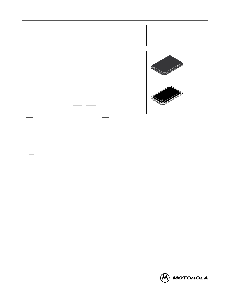
TQ PACKAGE
TQFP
CASE 983A–01
ZP PACKAGE
PBGA
CASE 999–02
REV 2
3/12/99
Motorola, Inc. 1999
相关PDF资料 |
PDF描述 |
|---|---|
| MCM69F536CTQ8.5 | 32K X 36 CACHE SRAM, 8.5 ns, PQFP100 |
| MCM93422PC | 256 X 4 STANDARD SRAM, 45 ns, PDIP22 |
| MCO100-16IO1 | |
| MCO150-16IO1 | |
| MCO75-12IO1 | |
相关代理商/技术参数 |
参数描述 |
|---|---|
| MCM63F819K | 制造商:FREESCALE 制造商全称:Freescale Semiconductor, Inc 功能描述:128K x 36 and 256K x 18 Bit Flow–Through BurstRAM Synchronous Fast Static RAM |
| MCM63F819KTQ11 | 制造商:FREESCALE 制造商全称:Freescale Semiconductor, Inc 功能描述:128K x 36 and 256K x 18 Bit Flow–Through BurstRAM Synchronous Fast Static RAM |
| MCM63F819KTQ11R | 制造商:FREESCALE 制造商全称:Freescale Semiconductor, Inc 功能描述:128K x 36 and 256K x 18 Bit Flow–Through BurstRAM Synchronous Fast Static RAM |
| MCM63F819KTQ8.5 | 制造商:FREESCALE 制造商全称:Freescale Semiconductor, Inc 功能描述:128K x 36 and 256K x 18 Bit Flow–Through BurstRAM Synchronous Fast Static RAM |
| MCM63F819KTQ8.5R | 制造商:FREESCALE 制造商全称:Freescale Semiconductor, Inc 功能描述:128K x 36 and 256K x 18 Bit Flow–Through BurstRAM Synchronous Fast Static RAM |
发布紧急采购,3分钟左右您将得到回复。