- 您现在的位置:买卖IC网 > PDF目录181824 > MCM63F737TQ9 (MOTOROLA INC) 128K X 36 CACHE SRAM, 9 ns, PQFP100 PDF资料下载
参数资料
| 型号: | MCM63F737TQ9 |
| 厂商: | MOTOROLA INC |
| 元件分类: | SRAM |
| 英文描述: | 128K X 36 CACHE SRAM, 9 ns, PQFP100 |
| 封装: | TQFP-100 |
| 文件页数: | 10/21页 |
| 文件大小: | 320K |
| 代理商: | MCM63F737TQ9 |
MCM63F737
MCM63F819
18
MOTOROLA FAST SRAM
APPLICATION INFORMATION
SLEEP MODE
A sleep mode feature, the ZZ pin, has been implemented
on the MCM63F737 and MCM63F819. It allows the system
designer to place the RAM in the lowest possible power
condition by asserting ZZ. The sleep mode timing diagram
shows the different modes of operation: Normal Operation,
No READ/WRITE Allowed, and Sleep Mode. Each mode has
its own set of constraints and conditions that are allowed.
Normal Operation: All inputs must meet setup and hold
times prior to sleep and tZZREC nanoseconds after re-
covering from sleep. Clock (K) must also meet cycle, high,
and low times during these periods. Two cycles prior to
sleep, initiation of either a read or write operation is not
allowed.
No READ/WRITE: During the period of time just prior to
sleep and during recovery from sleep, the assertion of either
ADSC, ADSP, or any write signal is not allowed. If a write
operation occurs during these periods, the memory array
may be corrupted. Validity of data out from the RAM can not
be guaranteed immediately after ZZ is asserted (prior to
being in sleep).
Sleep Mode: The RAM automatically deselects itself. The
RAM disconnects its internal clock buffer. The external clock
may continue to run without impacting the RAMs sleep
current (IZZ). All inputs are allowed to toggle — the RAM will
not be selected and perform any reads or writes. However, if
inputs toggle, the IZZ (max) specification will not be met.
Note: It is invalid to go from stop clock mode directly into
sleep mode.
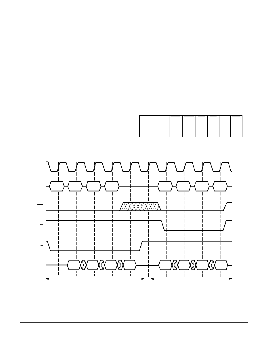
NON–BURST SYNCHRONOUS OPERATION
Although this BurstRAM has been designed for PowerPC
and other high end MPU–based systems, these SRAMs can
be used in other high speed L2 cache or memory applica-
tions that do not require the burst address feature. Most L2
caches designed with a synchronous interface can make use
of the MCM63F737 and MCM63F819. The burst counter fea-
ture of the BurstRAM can be disabled, and the SRAM can be
configured to act upon a continuous stream of addresses.
See Figure 6.
CONTROL PIN TIE VALUES EXAMPLE (H
≥ VIH, L ≤ VIL)
Non–Burst
ADSP
ADSC
ADV
SE1
SE2
LBO
Sync Non–Burst,
Flow–Through
SRAM
H
L
H
L
H
X
NOTE: Although X is specified in the table as a don’t care, the pin
must be tied either high or low.
WRITES
READS
DQ
K
Q(B)
Q(A)
ADDR
A
B
CD
EF
GH
W
Q(D)
Q(C)
D(E)
D(F)
D(G)
D(H)
G
Figure 6. Example Configuration as Non–Burst Synchronous SRAM
SE3
相关PDF资料 |
PDF描述 |
|---|---|
| MCM69F536CTQ8.5 | 32K X 36 CACHE SRAM, 8.5 ns, PQFP100 |
| MCM93422PC | 256 X 4 STANDARD SRAM, 45 ns, PDIP22 |
| MCO100-16IO1 | |
| MCO150-16IO1 | |
| MCO75-12IO1 | |
相关代理商/技术参数 |
参数描述 |
|---|---|
| MCM63F819K | 制造商:FREESCALE 制造商全称:Freescale Semiconductor, Inc 功能描述:128K x 36 and 256K x 18 Bit Flow–Through BurstRAM Synchronous Fast Static RAM |
| MCM63F819KTQ11 | 制造商:FREESCALE 制造商全称:Freescale Semiconductor, Inc 功能描述:128K x 36 and 256K x 18 Bit Flow–Through BurstRAM Synchronous Fast Static RAM |
| MCM63F819KTQ11R | 制造商:FREESCALE 制造商全称:Freescale Semiconductor, Inc 功能描述:128K x 36 and 256K x 18 Bit Flow–Through BurstRAM Synchronous Fast Static RAM |
| MCM63F819KTQ8.5 | 制造商:FREESCALE 制造商全称:Freescale Semiconductor, Inc 功能描述:128K x 36 and 256K x 18 Bit Flow–Through BurstRAM Synchronous Fast Static RAM |
| MCM63F819KTQ8.5R | 制造商:FREESCALE 制造商全称:Freescale Semiconductor, Inc 功能描述:128K x 36 and 256K x 18 Bit Flow–Through BurstRAM Synchronous Fast Static RAM |
发布紧急采购,3分钟左右您将得到回复。