- 您现在的位置:买卖IC网 > PDF目录296491 > MCM63P818ZP66 (FREESCALE SEMICONDUCTOR INC) 256K X 18 CACHE SRAM, 7 ns, PBGA119 PDF资料下载
参数资料
| 型号: | MCM63P818ZP66 |
| 厂商: | FREESCALE SEMICONDUCTOR INC |
| 元件分类: | SRAM |
| 英文描述: | 256K X 18 CACHE SRAM, 7 ns, PBGA119 |
| 封装: | 7 X 17 MM, PLASTIC, BGA-119 |
| 文件页数: | 5/21页 |
| 文件大小: | 451K |
| 代理商: | MCM63P818ZP66 |
MCM63P736
MCM63P818
13
MOTOROLA FAST SRAM
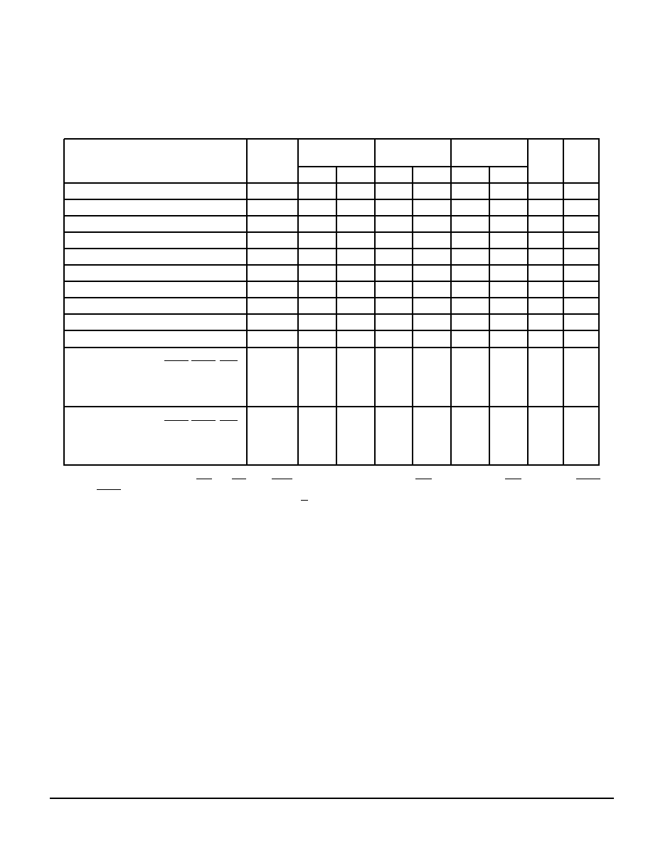
AC OPERATING CONDITIONS AND CHARACTERISTICS
(VDD = 3.3 V + 10%, – 5%, TA = 0 to 70°C, Unless Otherwise Noted)
Input Timing Measurement Reference Level
1.5 V
. . . . . . . . . . . . . . .
Input Pulse Levels
0 to 3.0 V
. . . . . . . . . . . . . . . . . . . . . . . . . . . . . . . . .
Input Rise/Fall Time
1.0 V/ns (20% to 80%)
. . . . . . . . . . . . . . . . . . . .
Output Timing Reference Level
1.5 V
. . . . . . . . . . . . . . . . . . . . . . . . . .
Output Load
See Figure 2 Unless Otherwise Noted
. . . . . . . . . . . . . .
READ/WRITE CYCLE TIMING (See Notes 1 and 2)
P
Sb l
MCM63P736–133
MCM63P818–133
MCM63P736–100
MCM63P818–100
MCM63P737–66
MCM63P819–66
Ui
N
Parameter
Symbol
Min
Max
Min
Max
Min
Max
Unit
Notes
Cycle Time
tKHKH
7.5
—
10
—
15
—
ns
Clock High Pulse Width
tKHKL
3
—
4
—
6
—
ns
3
Clock Low Pulse Width
tKLKH
3
—
4
—
6
—
ns
3
Clock Access Time
tKHQV
—
4
—
5
—
7
ns
Output Enable to Output Valid
tGLQV
—
3.8
—
4
—
6
ns
Clock High to Output Active
tKHQX1
0
—
0
—
0
—
ns
4, 5
Clock High to Output Change
tKHQX2
1.5
—
1.5
—
1.5
—
ns
4
Output Enable to Output Active
tGLQX
0
—
0
—
0
—
ns
4, 5
Output Disable to Q High–Z
tGHQZ
—
3.8
—
4
—
6
ns
4, 5
Clock High to Q High–Z
tKHQZ
1.5
7.5
1.5
10
1.5
15
ns
4, 5
Setup Times:
Address
ADSP, ADSC, ADV
Data In
Write
Chip Enable
tADKH
tADSKH
tDVKH
tWVKH
tEVKH
2
—
2
—
2
—
ns
Hold Times:
Address
ADSP, ADSC, ADV
Data In
Write
Chip Enable
tKHAX
tKHADSX
tKHDX
tKHWX
tKHEX
0.5
—
0.5
—
0.5
—
ns
NOTES:
1. Write is defined as either any SBx and SW low or SGW is low. Chip Enable is defined as SE1 low, SE2 high, and SE3 low whenever ADSP
or ADSC is asserted.
2. All read and write cycle timings are referenced from K or G.
3. In order to reduce test correlation issues and to reduce the effects of application specific input edge rate variations on correlation between
data sheet parameters and actual system performance, FSRAM AC parametric specifications are always specified at VDDQ/2. In some
design exercises, it is desirable to evaluate timing using other reference levels. Since the maximum test input edge rate is known and is
given in the AC Test Conditions section of the data sheet as 1 V/ns, one can easily interpolate timing values to other reference levels.
4. This parameter is sampled and not 100% tested.
5. Measured at
± 200 mV from steady state.
F
re
e
sc
a
le
S
e
m
ic
o
n
d
u
c
to
r,
I
Freescale Semiconductor, Inc.
For More Information On This Product,
Go to: www.freescale.com
n
c
..
.
AR
CH
IVE
D B
Y F
RE
ES
CA
LE
SE
MI
CO
ND
UC
TO
R,
INC
.
相关PDF资料 |
PDF描述 |
|---|---|
| MCM69F737ZP8 | 128K X 36 CACHE SRAM, 8 ns, PBGA119 |
| MCO15DAG-FREQ-OUT21-V1 | CRYSTAL OSCILLATOR, CLOCK, 0.000732 MHz - 6 MHz, CMOS OUTPUT |
| MCO15DCG-FREQ-OUT21-V1 | CRYSTAL OSCILLATOR, CLOCK, 0.000732 MHz - 3 MHz, CMOS OUTPUT |
| MCO16DAG-FREQ-OUT21-V2 | CRYSTAL OSCILLATOR, CLOCK, 0.000732 MHz - 12 MHz, CMOS OUTPUT |
| MCO21CCG-3MHZ-OUT21-V2 | CRYSTAL OSCILLATOR, CLOCK, 3 MHz, CMOS OUTPUT |
相关代理商/技术参数 |
参数描述 |
|---|---|
| MCM63P818ZP66R | 制造商:MOTOROLA 制造商全称:Motorola, Inc 功能描述:128K x 36 and 256K x 18 Bit Pipelined BurstRAM Synchronous Fast Static RAM |
| MCM63P837 | 制造商:MOTOROLA 制造商全称:Motorola, Inc 功能描述:256K x 36 and 512K x 18 Bit Pipelined BurstRAM Synchronous Fast Static RAM |
| MCM63R836 | 制造商:FREESCALE 制造商全称:Freescale Semiconductor, Inc 功能描述:MCM63R836 |
| MCM63R836A | 制造商:FREESCALE 制造商全称:Freescale Semiconductor, Inc 功能描述:8M Late Write HSTL |
| MCM63R836FC3.0 | 制造商:FREESCALE 制造商全称:Freescale Semiconductor, Inc 功能描述:MCM63R836 |
发布紧急采购,3分钟左右您将得到回复。