- 您现在的位置:买卖IC网 > PDF目录5091 > MCP1700-2702E/TO (Microchip Technology)IC REG LDO 2.7V .25A TO-92-3 PDF资料下载
参数资料
| 型号: | MCP1700-2702E/TO |
| 厂商: | Microchip Technology |
| 文件页数: | 3/24页 |
| 文件大小: | 0K |
| 描述: | IC REG LDO 2.7V .25A TO-92-3 |
| 标准包装: | 1,000 |
| 稳压器拓扑结构: | 正,固定式 |
| 输出电压: | 2.7V |
| 输入电压: | 最高 6V |
| 电压 - 压降(标准): | 0.178V @ 250mA |
| 稳压器数量: | 1 |
| 电流 - 输出: | 250mA(最小) |
| 工作温度: | -40°C ~ 125°C |
| 安装类型: | 通孔 |
| 封装/外壳: | TO-226-3、TO-92-3 标准主体 |
| 供应商设备封装: | TO-92-3 |
| 包装: | 散装 |
�� �
�
�MCP1700�
�1.0�
�ELECTRICAL�
�CHARACTERISTICS�
�?� Notice:� Stresses� above� those� listed� under� “Maximum�
�Ratings”� may� cause� permanent� damage� to� the� device.� This� is�
�a� stress� rating� only� and� functional� operation� of� the� device� at�
�those� or� any� other� conditions� above� those� indicated� in� the�
�Absolute� Maximum� Ratings� ?�
�V� DD� ............................................................................................+� 6.5V�
�All� inputs� and� outputs� w.r.t.� .............(V� SS� -0.3V)� to� (V� IN� +0.3V)�
�Peak� Output� Current� ....................................� Internally� Limited�
�operational� listings� of� this� specification� is� not� implied.�
�Exposure� to� maximum� rating� conditions� for� extended� periods�
�may� affect� device� reliability.�
�Storage� temperature� .....................................-65°C� to� +150°C�
�Maximum� Junction� Temperature� ...................................� 150°C�
�Operating� Junction� Temperature...................-40°C� to� +125°C�
�ESD� protection� on� all� pins� (HBM;MM)� ...............� ≥� 4� kV;� ≥� 400V�
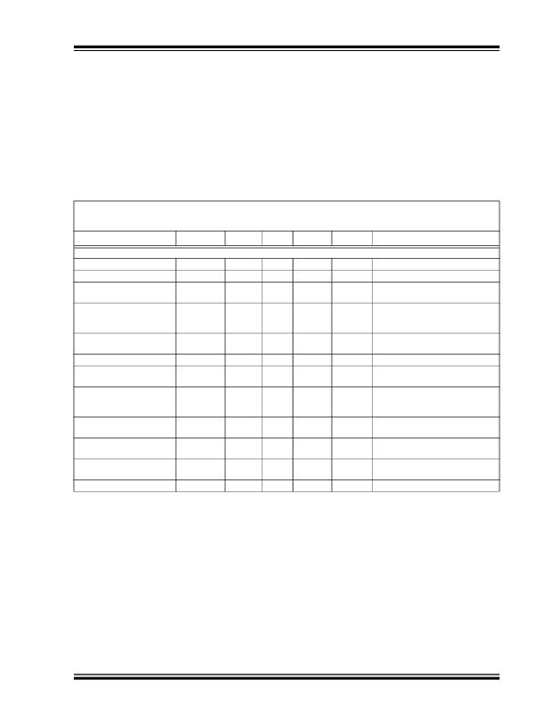
�DC� CHARACTERISTICS�
�Electrical� Characteristics:� Unless� otherwise� specified,� all� limits� are� established� for� V� IN� =� V� R� +� 1,� I� LOAD� =� 100� μA,�
�C� OUT� =� 1� μF� (X7R),� C� IN� =� 1� μF� (X7R),� T� A� =� +25°C.�
�Boldface� type� applies� for� junction� temperatures,� T� J� (Note� 6)� of� -40°C� to� +125°C.�
�Parameters�
�Sym�
�Min�
�Typ�
�Max�
�Units�
�Conditions�
�Input� /� Output� Characteristics�
�Input� Operating� Voltage�
�Input� Quiescent� Current�
�Maximum� Output� Current�
�Output� Short� Circuit� Current�
�V� IN�
�I� q�
�I� OUT_mA�
�I� OUT_SC�
�2.3�
�—�
�250�
�200�
�—�
�—�
�1.6�
�—�
�—�
�408�
�6.0�
�4�
�—�
�—�
�—�
�V�
�μA�
�mA�
�mA�
��I� L� =� 0� mA,� V� IN� =� V� R� +1V�
�For� V� R� ≥� 2.5V�
�For� V� R� <� 2.5V�
�V� IN� =� V� R� +� V,� V� OUT� =� GND,�
�Current� (peak� current)� measured�
�10� ms� after� short� is� applied.�
�Output� Voltage� Regulation�
�V� OUT� Temperature� Coefficient�
�Line� Regulation�
�Load� Regulation�
�Dropout� Voltage�
�V� R� >� 2.5V�
�Dropout� Voltage�
�V� R� <� 2.5V�
�Output� Rise� Time�
�V� OUT�
�TCV� OUT�
�Δ� V� OUT� /�
�(V� OUT� X� Δ� V� IN� )�
�Δ� V� OUT� /V� OUT�
�V� IN� -V� OUT�
�V� IN� -V� OUT�
�T� R�
�V� R� -3.0%�
�V� R� -2.0%�
�—�
�-1.0�
�-1.5�
�—�
�—�
�—�
�V� R� ±0.4�
�%�
�50�
�±0.75�
�±1.0�
�178�
�150�
�500�
�V� R� +3.0%�
�V� R� +2.0%�
�—�
�+1.0�
�+1.5�
�350�
�350�
�—�
�V�
�ppm/°C�
�%/V�
�%�
�mV�
�mV�
�μs�
���(V� R� +1)V� ≤� V� IN� ≤� 6V�
�I� L� =� 0.1� mA� to� 250� mA� for� V� R� ≥� 2.5V�
�I� L� =� 0.1� mA� to� 200� mA� for� V� R� <� 2.5V�
����10%� V� R� to� 90%� V� R� V� IN� =� 0V� to� 6V,�
�R� L� =� 50� Ω� resistive�
�Output� Noise�
�e� N�
�—�
�3�
�—�
�μV/(Hz)� 1/2� I� L� =� 100� mA,� f� =� 1� kHz,� C� OUT� =� 1� μF�
�Note� 1:�
�2:�
�3:�
�4:�
�5:�
�6:�
�7:�
�The� minimum� V� IN� must� meet� two� conditions:� V� IN� ≥� 2.3V� and� V� IN� ≥� (� V� R� +� 3.0%� )� +� V� DROPOUT� .�
�V� R� is� the� nominal� regulator� output� voltage.� For� example:� V� R� =� 1.2V,� 1.5V,� 1.8V,� 2.5V,� 2.8V,� 3.0V,� 3.3V,� 4.0V,� 5.0V.� The�
�input� voltage� (V� IN� =� V� R� +� 1.0V);� I� OUT� =� 100� μA.�
�TCV� OUT� =� (V� OUT-HIGH� -� V� OUT-LOW� )� *10� 6� /� (V� R� *� Δ� Temperature),� V� OUT-HIGH� =� highest� voltage� measured� over� the�
�temperature� range.� V� OUT-LOW� =� lowest� voltage� measured� over� the� temperature� range.�
�Load� regulation� is� measured� at� a� constant� junction� temperature� using� low� duty� cycle� pulse� testing.� Changes� in� output�
�voltage� due� to� heating� effects� are� determined� using� thermal� regulation� specification� TCV� OUT� .�
�Dropout� voltage� is� defined� as� the� input� to� output� differential� at� which� the� output� voltage� drops� 2%� below� its� measured�
�value� with� a� V� R� +� 1V� differential� applied.�
�The� maximum� allowable� power� dissipation� is� a� function� of� ambient� temperature,� the� maximum� allowable� junction�
�temperature� and� the� thermal� resistance� from� junction� to� air� (i.e.,� T� A� ,� T� J� ,� θ� JA� ).� Exceeding� the� maximum� allowable� power�
�dissipation� will� cause� the� device� operating� junction� temperature� to� exceed� the� maximum� 150°C� rating.� Sustained�
�junction� temperatures� above� 150°C� can� impact� the� device� reliability.�
�The� junction� temperature� is� approximated� by� soaking� the� device� under� test� at� an� ambient� temperature� equal� to� the�
�desired� Junction� temperature.� The� test� time� is� small� enough� such� that� the� rise� in� the� Junction� temperature� over� the�
�ambient� temperature� is� not� significant.�
�?� 2007� Microchip� Technology� Inc.�
�DS21826B-page� 3�
�相关PDF资料 |
PDF描述 |
|---|---|
| EEV-HB1V220P | CAP ALUM 22UF 35V 20% SMD |
| GCC50DREN-S734 | CONN EDGECARD 100PS .100 EYELET |
| MCP1700-2302E/TO | IC REG LDO 2.3V .2A TO-92-3 |
| GCC50DREH-S734 | CONN EDGECARD 100PS .100 EYELET |
| MCP1700-2202E/TO | IC REG LDO 2.2V .2A TO-92-3 |
相关代理商/技术参数 |
参数描述 |
|---|---|
| MCP1700-2802E/TO | 功能描述:低压差稳压器 - LDO 250mA CMOS LDO Isupp 1uA 2% Vout Acc RoHS:否 制造商:Texas Instruments 最大输入电压:36 V 输出电压:1.4 V to 20.5 V 回动电压(最大值):307 mV 输出电流:1 A 负载调节:0.3 % 输出端数量: 输出类型:Fixed 最大工作温度:+ 125 C 安装风格:SMD/SMT 封装 / 箱体:VQFN-20 |
| MCP1700-3001E/TO | 功能描述:低压差稳压器 - LDO 250mA CMOS LDO Isupp 1uA 2% Vout Acc RoHS:否 制造商:Texas Instruments 最大输入电压:36 V 输出电压:1.4 V to 20.5 V 回动电压(最大值):307 mV 输出电流:1 A 负载调节:0.3 % 输出端数量: 输出类型:Fixed 最大工作温度:+ 125 C 安装风格:SMD/SMT 封装 / 箱体:VQFN-20 |
| MCP1700-3002E/MB | 制造商:Microchip Technology Inc 功能描述: |
| MCP1700-3002E/TO | 功能描述:低压差稳压器 - LDO 250mA Adj LDO 2% RoHS:否 制造商:Texas Instruments 最大输入电压:36 V 输出电压:1.4 V to 20.5 V 回动电压(最大值):307 mV 输出电流:1 A 负载调节:0.3 % 输出端数量: 输出类型:Fixed 最大工作温度:+ 125 C 安装风格:SMD/SMT 封装 / 箱体:VQFN-20 |
| MCP1700-3102E/TO | 功能描述:低压差稳压器 - LDO 250mA CMOS LDO Isupp 1uA 2% Vout Acc RoHS:否 制造商:Texas Instruments 最大输入电压:36 V 输出电压:1.4 V to 20.5 V 回动电压(最大值):307 mV 输出电流:1 A 负载调节:0.3 % 输出端数量: 输出类型:Fixed 最大工作温度:+ 125 C 安装风格:SMD/SMT 封装 / 箱体:VQFN-20 |
发布紧急采购,3分钟左右您将得到回复。