- 您现在的位置:买卖IC网 > PDF目录9044 > MCP4725A1T-E/CH (Microchip Technology)IC DAC 12BIT EE W/I2C SOT23-6 PDF资料下载
参数资料
| 型号: | MCP4725A1T-E/CH |
| 厂商: | Microchip Technology |
| 文件页数: | 11/50页 |
| 文件大小: | 0K |
| 描述: | IC DAC 12BIT EE W/I2C SOT23-6 |
| 标准包装: | 1 |
| 设置时间: | 6µs |
| 位数: | 12 |
| 数据接口: | EEPROM,I²C,串行 |
| 转换器数目: | 1 |
| 电压电源: | 单电源 |
| 工作温度: | -40°C ~ 125°C |
| 安装类型: | 表面贴装 |
| 封装/外壳: | SOT-23-6 |
| 供应商设备封装: | SOT-23-6 |
| 包装: | 标准包装 |
| 输出数目和类型: | 1 电压,单极;1 电压,双极 |
| 采样率(每秒): | * |
| 产品目录页面: | 673 (CN2011-ZH PDF) |
| 配用: | MCP4725DM-PTPLS-ND - BOARD DAUGHTER PICTAIL MCP4725 |
| 其它名称: | MCP4725A1T-E/CHDKR |
第1页第2页第3页第4页第5页第6页第7页第8页第9页第10页当前第11页第12页第13页第14页第15页第16页第17页第18页第19页第20页第21页第22页第23页第24页第25页第26页第27页第28页第29页第30页第31页第32页第33页第34页第35页第36页第37页第38页第39页第40页第41页第42页第43页第44页第45页第46页第47页第48页第49页第50页
2009 Microchip Technology Inc.
DS22039D-page 19
MCP4725
5.0
GENERAL DESCRIPTION
The MCP4725 is a single channel buffered voltage
output
12-bit
DAC
with
non-volatile
memory
(EEPROM). The user can store configuration register
bits (2 bits) and DAC input data (12 bits) in non-volatile
EEPROM (14 bits) memory.
When the device is powered on first, it loads the DAC
code from the EEPROM and outputs the analog output
accordingly with the programmed settings. The user
can reprogram the EEPROM or DAC register any time.
The device uses a resistor string architecture. DAC’s
output is buffered with a low power precision amplifier.
This output amplifier provides low offset voltage and
low noise, as well as rail-to-rail output. The amplifier
can also provide high source currents (VOUT pin to
VSS).
The DAC can be configured to normal or power saving
power-down mode by setting the configuration register
bits.
The device uses a two-wire I2C compatible serial
interface and operates from a single power supply
ranging from 2.7V to 5.5V.
5.1
Output Voltage
The input coding to the MCP4725 device is unsigned
binary. The output voltage range is from 0V to VDD. The
output voltage is given in Equation 5-1:
EQUATION 5-1:
5.1.1
OUTPUT AMPLIFIER
The DAC output is buffered with a low-power, precision
CMOS amplifier. This amplifier provides low offset
voltage and low noise. The output stage enables the
device to operate with output voltages close to the
power supply rails. Refer to Section 1.0 “Electrical
Characteristics” for range and load conditions.
The output amplifier can drive the resistive and high
capacitive loads without oscillation. The amplifier can
provide maximum load current as high as 25 mA which
is enough for most of a programmable voltage
reference applications.
5.1.2
DRIVING RESISTIVE AND
CAPACITIVE LOADS
The MCP4725 output stage is capable of driving loads
up to 1000 pF in parallel with 5 k load resistance.
drops slowly as the load resistance decreases after
about 3.5 k.
5.2
LSB SIZE
One LSB is defined as the ideal voltage difference
between two successive codes. (see Equation 4-1).
Table 5-1 shows an example of the LSB size over full
scale range (VDD).
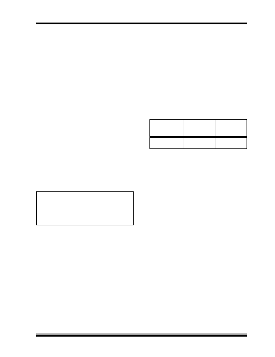
TABLE 5-1:
LSB SIZES FOR MCP4725
(EXAMPLE)
5.3
Voltage Reference
The MCP4725 device uses the VDD as its voltage
reference. Any variation or noises on the VDD line can
affect directly on the DAC output. The VDD needs to be
as clean as possible for accurate DAC performance.
5.4
Reset Conditions
In the Reset conditions, the device uploads the
EEPROM data into the DAC register. The device can
be reset by two independent events: (a) by POR or (b)
by I2C General Call Reset Command.
The factory default settings for the EEPROM prior to
shipment are shown in Table 5-3 (set for a middle scale
output). The user can rewrite or read the DAC register
or EEPROM anytime after the Power-On-Reset event.
5.4.1
POWER-ON-RESET
The device’s internal Power-On-Reset (POR) circuit
ensures that the device powers up in a defined state.
If the power supply voltage is less than the POR thresh-
old (VPOR = 2V, typical), all circuits are disabled and
there will be no DAC output. When the VDD increases
above the VPOR, the device takes a reset state. During
the reset period, the device uploads all configuration
and DAC input codes from EEPROM. The DAC output
will be the same as for the value last stored in the
EEPROM. This enables the device returns to the same
state that it was at the last write to the EEPROM before
it was powered off.
V
OUT
V
REF
D
n
×
()
4096
-------------------------------
=
Where:
VREF
=VDD
Dn
=
Input code
Full Scale
Range
(VDD)
LSB
Size
Condition
3.0V
0.73 mV
3V / 4096
5.0V
1.22 mV
5V / 4096
相关PDF资料 |
PDF描述 |
|---|---|
| M83723/95A1404N | CONN PLUG 4POS STRAIGHT W/SCKT |
| VI-BTH-MY-F1 | CONVERTER MOD DC/DC 52V 50W |
| VI-BTF-MY-F4 | CONVERTER MOD DC/DC 72V 50W |
| MS27496E13B4P | CONN RCPT 4POS BOX MNT W/PINS |
| MCP4725A0T-E/CH | IC DAC 12BIT W/I2C SOT23A-6 |
相关代理商/技术参数 |
参数描述 |
|---|---|
| MCP4725A2T-E/CH | 功能描述:数模转换器- DAC Sngl 12-B NV DAC w/ I2C interface RoHS:否 制造商:Texas Instruments 转换器数量:1 DAC 输出端数量:1 转换速率:2 MSPs 分辨率:16 bit 接口类型:QSPI, SPI, Serial (3-Wire, Microwire) 稳定时间:1 us 最大工作温度:+ 85 C 安装风格:SMD/SMT 封装 / 箱体:SOIC-14 封装:Tube |
| MCP4725A2T-E/CH-CUT TAPE | 制造商:Microchip 功能描述:MCP4725 Series 1 Ch I2C EEPROM Memory 5.5 V 12-Bit D/A Converter SMT - SOT-23-6 |
| MCP4725A3T-E/CH | 功能描述:数模转换器- DAC Sngl 12-B NV DAC w/ I2C interface RoHS:否 制造商:Texas Instruments 转换器数量:1 DAC 输出端数量:1 转换速率:2 MSPs 分辨率:16 bit 接口类型:QSPI, SPI, Serial (3-Wire, Microwire) 稳定时间:1 us 最大工作温度:+ 85 C 安装风格:SMD/SMT 封装 / 箱体:SOIC-14 封装:Tube |
| MCP4725A3T-E/CH-CUT TAPE | 制造商:Microchip 功能描述:MCP4725 Series 1 Ch I2C EEPROM Memory 5.5 V 12-Bit D/A Converter SMT - SOT-23-6 |
| MCP4725DM-PTPLS | 功能描述:子卡和OEM板 MCP4725 DAC PICTail Plus Daughter Board RoHS:否 制造商:BeagleBoard by CircuitCo 产品:BeagleBone LCD4 Boards 用于:BeagleBone - BB-Bone - Open Source Development Kit |
发布紧急采购,3分钟左右您将得到回复。