参数资料
| 型号: | MCP659T-E/ML |
| 厂商: | Microchip Technology |
| 文件页数: | 16/66页 |
| 文件大小: | 0K |
| 描述: | IC OP AMP 50MHZ RRIO 16QFN |
| 标准包装: | 3,300 |
| 系列: | mCal 技术 |
| 放大器类型: | 通用 |
| 电路数: | 4 |
| 输出类型: | 满摆幅 |
| 转换速率: | 30 V/µs |
| 增益带宽积: | 50MHz |
| 电流 - 输入偏压: | 6pA |
| 电压 - 输入偏移: | 200µV |
| 电流 - 电源: | 6mA |
| 电流 - 输出 / 通道: | 150mA |
| 电压 - 电源,单路/双路(±): | 2.5 V ~ 5.5 V |
| 工作温度: | -40°C ~ 125°C |
| 安装类型: | 表面贴装 |
| 封装/外壳: | 16-VQFN 裸露焊盘 |
| 供应商设备封装: | 16-QFN(4x4) |
| 包装: | 带卷 (TR) |
第1页第2页第3页第4页第5页第6页第7页第8页第9页第10页第11页第12页第13页第14页第15页当前第16页第17页第18页第19页第20页第21页第22页第23页第24页第25页第26页第27页第28页第29页第30页第31页第32页第33页第34页第35页第36页第37页第38页第39页第40页第41页第42页第43页第44页第45页第46页第47页第48页第49页第50页第51页第52页第53页第54页第55页第56页第57页第58页第59页第60页第61页第62页第63页第64页第65页第66页
2009-2011 Microchip Technology Inc.
DS22146C-page 23
MCP651/1S/2/3/4/5/9
4.0
APPLICATIONS
The MCP651/1S/2/3/4/5/9 family of self-zeroed op
amps
is
manufactured
using
Microchip’s
state-of-the-art CMOS process. It is designed for
low-cost, low-power and high precision applications. Its
low supply voltage, low quiescent current and wide
bandwidth makes the MCP651/1S/2/3/4/5/9 ideal for
battery-powered applications.
4.1
Calibration and Chip Select
These op amps include circuitry for dynamic calibration
of the offset voltage (VOS).
4.1.1
mCal CALIBRATION CIRCUITRY
The internal mCal circuitry, when activated, starts a
delay timer (to wait for the op amp to settle to its new
bias point), then calibrates the input offset voltage
(VOS). The mCal circuitry is triggered at power-up (and
after some power brown-out events) by the internal
POR, and by the memory’s Parity Detector. The
power-up time, when the mCal circuitry triggers the cal-
ibration sequence, is 200 ms (typical).
4.1.2
CAL/CS PIN
The CAL/CS pin gives the user a means to externally
demand a Low-Power mode of operation, then to
calibrate VOS. Using the CAL/CS pin makes it possible
to correct VOS as it drifts over time (1/f noise and aging;
see Figure 2-35) and across temperature.
The CAL/CS pin performs two functions: it places the
op amp(s) in a Low-Power mode when it is held high,
and starts a calibration event (correction of VOS) after a
rising edge.
While in the Low-Power mode, the quiescent current is
quite small (ISS = -3 A, typical). The output is also in a
High-Z state.
During the calibration event, the quiescent current is
near, but smaller than, the specified quiescent current
(6 mA, typical). The output continues in the High-Z
state, and the inputs are disconnected from the
external circuit, to prevent internal signals from
affecting circuit operation. The op amp inputs are
internally connected to a Common mode voltage buffer
and feedback resistors. The offset is corrected (using a
digital state machine, logic and memory), and the
calibration constants are stored in memory.
Once the calibration event is completed, the amplifier is
reconnected to the external circuitry. The turn-on time,
when calibration is started with the CAL/CS pin, is 3 ms
(typical).
There is an internal 5 M
pull-down resistor tied to the
CAL/CS pin. If the CAL/CS pin is left floating, the
amplifier operates normally.
For the MCP655 dual and the MCP659 quad, there is
an additional constraint on toggling the two CAL/CS
pins close together; see the t
CON specification in
Table 1-3. If the two pins are toggled simultaneously, or
if they are toggled separately with an adequate delay
between them (greater than t
CON), then the CAL/CS
inputs are accepted as valid. If one of the two pins
toggles while the other pin’s calibration routine is in
progress, then an invalid input occurs and the result is
unpredictable.
4.1.3
INTERNAL POR
This part includes an internal Power-on Reset (POR) to
protect the internal calibration memory cells. The POR
monitors the power supply voltage (VDD). When the
POR detects a low VDD event, it places the part into the
Low-Power mode of operation. When the POR detects
a normal VDD event, it starts a delay counter, then trig-
gers an calibration event. The additional delay gives a
total POR turn-on time of 200 ms (typical); this is also
the power-up time (since the POR is triggered at
power-up).
4.1.4
PARITY DETECTOR
A parity error detector monitors the memory contents
for any corruption. In the rare event that a parity error is
detected (e.g., corruption from an alpha particle), a
POR event is automatically triggered. This will cause
the input offset voltage to be re-corrected, and the op
amp will not return to normal operation for a period of
time (the POR turn-on time, tPON).
4.1.5
CALIBRATION INPUT PIN
A VCAL pin is available in some options (e.g., the single
MCP651) for those applications that need the
calibration to occur at an internally driven Common
mode voltage other than VDD/3.
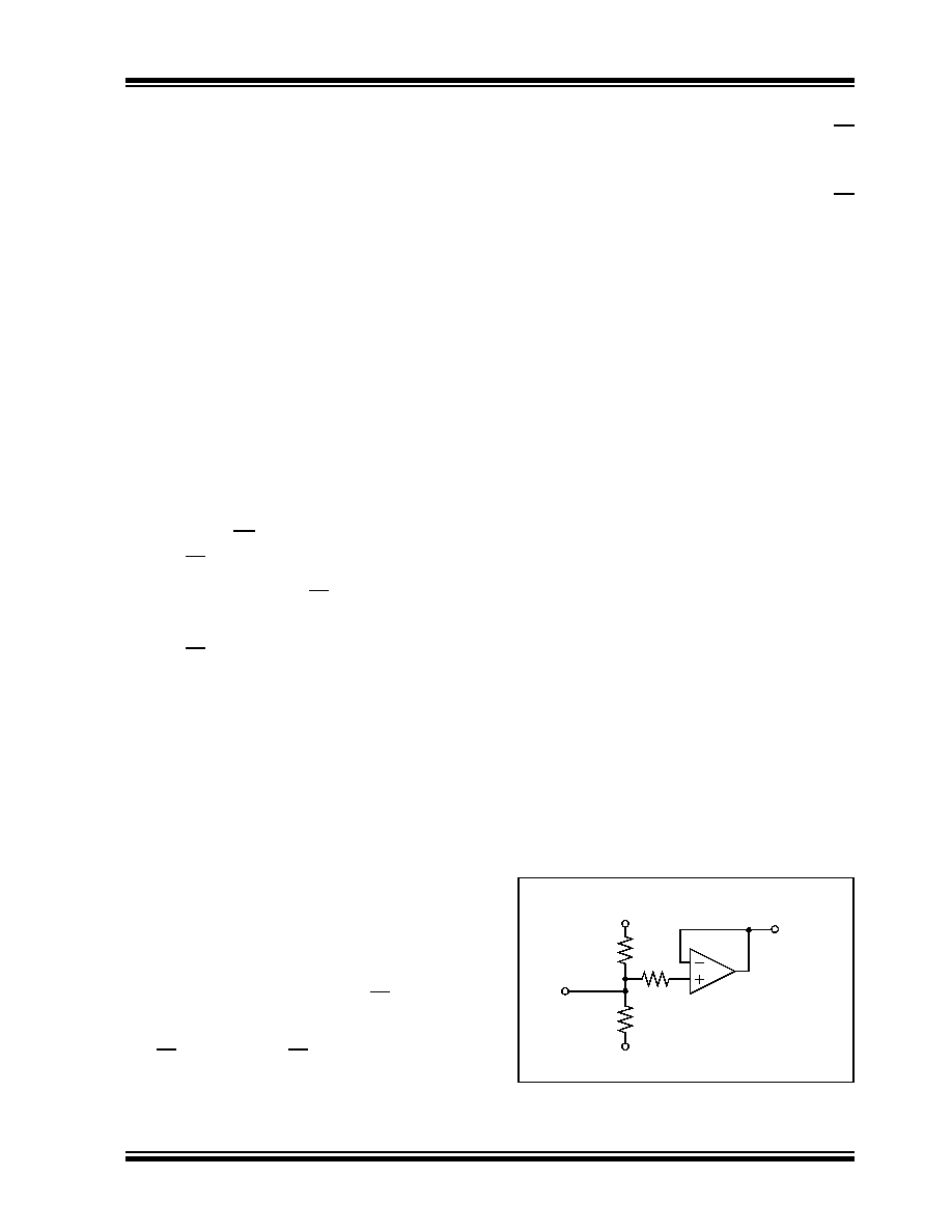
Figure 4-1 shows the reference circuit that internally
sets the op amp’s Common mode reference voltage
(VCM_INT) during calibration (the resistors are
disconnected from the supplies at other times). The
5k
resistor provides over-current protection for the
buffer.
FIGURE 4-1:
Common-Mode Reference’s
Input Circuitry.
To op amp during
VCAL
BUFFER
5k
300 k
150 k
VSS
VDD
calibration
VCM_INT
相关PDF资料 |
PDF描述 |
|---|---|
| MCP662-E/MS | IC OP AMP 60MHZ DUAL 8-MSOP |
| MCP669T-E/ML | IC OPAMP QUAD 60MHZ 16QFN |
| MCP6H04T-E/SL | IC OPAMP QUAD16V 1.2MHZ 14SOIC |
| MCP6N11T-100E/SN | IC AMP INSTR RRIO 35MHZ 8SOIC |
| MCP6V11T-E/OT | IC OPAMP SGL ZERO DRIFT SOT23-5 |
相关代理商/技术参数 |
参数描述 |
|---|---|
| MCP65R41T-1202E/CHY | 功能描述:校验器 IC Single Push/Pull Comparator 1.2V Ref RoHS:否 制造商:STMicroelectronics 产品: 比较器类型: 通道数量: 输出类型:Push-Pull 电源电压-最大:5.5 V 电源电压-最小:1.1 V 补偿电压(最大值):6 mV 电源电流(最大值):1350 nA 响应时间: 最大工作温度:+ 125 C 安装风格:SMD/SMT 封装 / 箱体:SC-70-5 封装:Reel |
| MCP65R41T-2402E/CHY | 功能描述:校验器 IC Single Push/Pull Comparator 2.4V Ref RoHS:否 制造商:STMicroelectronics 产品: 比较器类型: 通道数量: 输出类型:Push-Pull 电源电压-最大:5.5 V 电源电压-最小:1.1 V 补偿电压(最大值):6 mV 电源电流(最大值):1350 nA 响应时间: 最大工作温度:+ 125 C 安装风格:SMD/SMT 封装 / 箱体:SC-70-5 封装:Reel |
| MCP65R46T-1202E/CHY | 功能描述:校验器 IC Single Open Drain Comparator 1.2V Ref RoHS:否 制造商:STMicroelectronics 产品: 比较器类型: 通道数量: 输出类型:Push-Pull 电源电压-最大:5.5 V 电源电压-最小:1.1 V 补偿电压(最大值):6 mV 电源电流(最大值):1350 nA 响应时间: 最大工作温度:+ 125 C 安装风格:SMD/SMT 封装 / 箱体:SC-70-5 封装:Reel |
| MCP65R46T-2402E/CHY | 功能描述:校验器 IC Single Open Drain Comparator 2.4V Ref RoHS:否 制造商:STMicroelectronics 产品: 比较器类型: 通道数量: 输出类型:Push-Pull 电源电压-最大:5.5 V 电源电压-最小:1.1 V 补偿电压(最大值):6 mV 电源电流(最大值):1350 nA 响应时间: 最大工作温度:+ 125 C 安装风格:SMD/SMT 封装 / 箱体:SC-70-5 封装:Reel |
| MCP660-E/ML | 功能描述:运算放大器 - 运放 Triple 60MHz OP w/CS E temp RoHS:否 制造商:STMicroelectronics 通道数量:4 共模抑制比(最小值):63 dB 输入补偿电压:1 mV 输入偏流(最大值):10 pA 工作电源电压:2.7 V to 5.5 V 安装风格:SMD/SMT 封装 / 箱体:QFN-16 转换速度:0.89 V/us 关闭:No 输出电流:55 mA 最大工作温度:+ 125 C 封装:Reel |
发布紧急采购,3分钟左右您将得到回复。