- 您现在的位置:买卖IC网 > PDF目录67988 > MCV18E-I/P 32-BIT, FLASH, 20 MHz, RISC MICROCONTROLLER, PDIP18 PDF资料下载
参数资料
| 型号: | MCV18E-I/P |
| 元件分类: | 微控制器/微处理器 |
| 英文描述: | 32-BIT, FLASH, 20 MHz, RISC MICROCONTROLLER, PDIP18 |
| 封装: | 0.300 INCH, LEAD FREE, PLASTIC, DIP-18 |
| 文件页数: | 95/108页 |
| 文件大小: | 1509K |
| 代理商: | MCV18E-I/P |
第1页第2页第3页第4页第5页第6页第7页第8页第9页第10页第11页第12页第13页第14页第15页第16页第17页第18页第19页第20页第21页第22页第23页第24页第25页第26页第27页第28页第29页第30页第31页第32页第33页第34页第35页第36页第37页第38页第39页第40页第41页第42页第43页第44页第45页第46页第47页第48页第49页第50页第51页第52页第53页第54页第55页第56页第57页第58页第59页第60页第61页第62页第63页第64页第65页第66页第67页第68页第69页第70页第71页第72页第73页第74页第75页第76页第77页第78页第79页第80页第81页第82页第83页第84页第85页第86页第87页第88页第89页第90页第91页第92页第93页第94页当前第95页第96页第97页第98页第99页第100页第101页第102页第103页第104页第105页第106页第107页第108页
2009 Microchip Technology Inc.
DS41399A-page 87
MCV18E
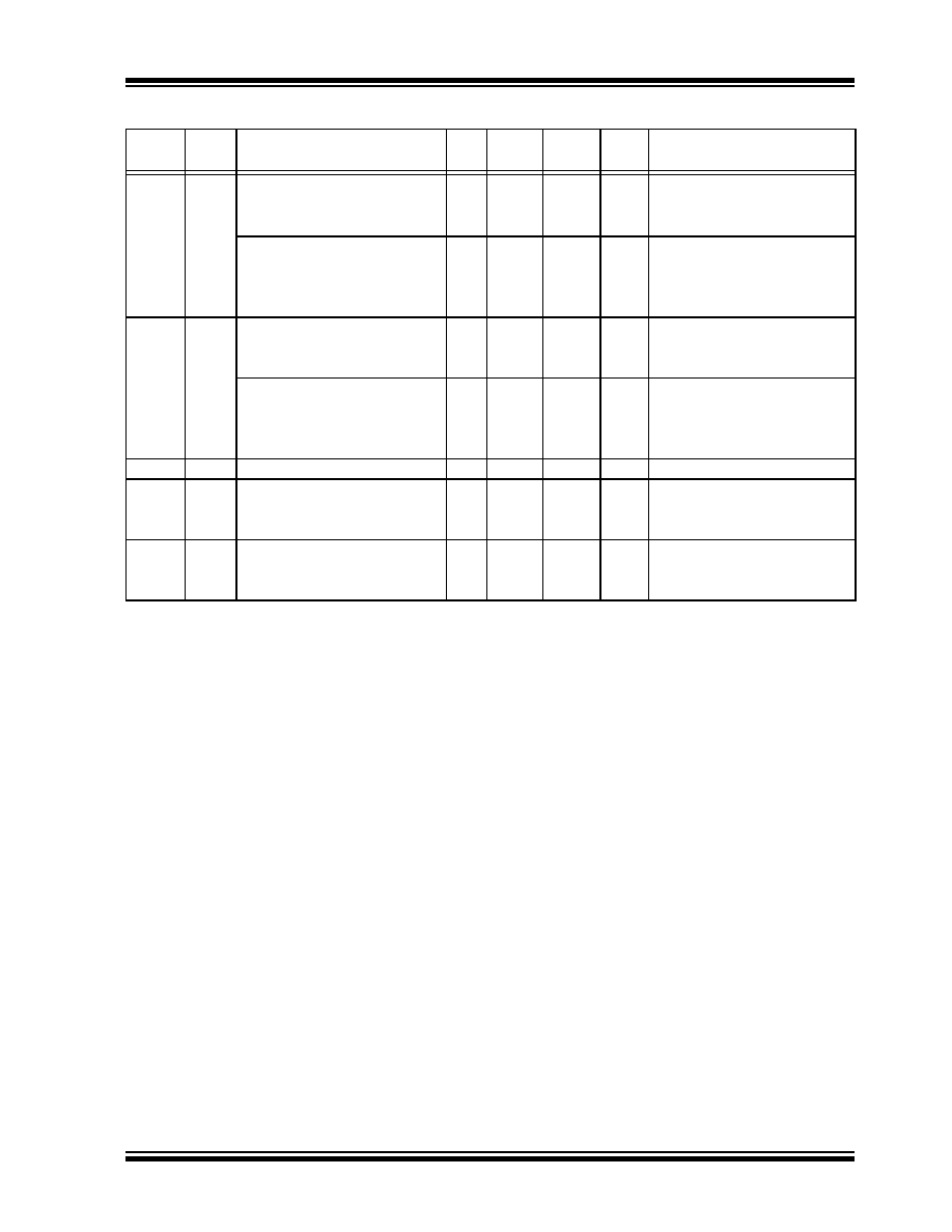
TABLE 10-2:
EXTERNAL CLOCK TIMING REQUIREMENTS
Param
No.
Sym
Characteristic
Min
Typ
Max
Units
Conditions
1A
FOSC
Ext. Clock Input Frequency(1)
DC
—
4
MHz RC and XT Osc modes
DC
—
20
MHz HS Osc mode
DC
—
200
kHz
LP Osc mode
Oscillator Frequency(1)
DC
—
4
MHz RC Osc mode
0.1
—
4
MHz XT Osc mode
4
—
20
MHz HS Osc mode
5
—
200
kHz
LP Osc mode
1TOSC
External CLKIN Period(1)
250
—
ns
RC and XT Osc modes
50
—
ns
HS Osc mode
5—
—
μs
LP Osc mode
Oscillator Period(1)
250
—
ns
RC Osc mode
250
—
10,000
ns
XT Osc mode
50
—
250
ns
HS Osc mode
5—
—
μs
LP Osc mode
2
Tcy
Instruction Cycle Time(1)
200
—
DC
ns
TCY = 4/FOSC
3*
TosL,
TosH
External Clock in (OSC1) High or
Low Time
100
—
ns
XT oscillator
2.5
—
μs
LP oscillator
15
—
ns
HS oscillator
4*
TosR,
TosF
External Clock in (OSC1) Rise or
Fall Time
—
25
ns
XT oscillator
—
50
ns
LP oscillator
—
15
ns
HS oscillator
*
These parameters are characterized but not tested.
Data in “Typ” column is at 5V, 25°C unless otherwise stated. These parameters are for design guidance
only and are not tested.
Note 1:
Instruction cycle period (TCY) equals four times the input oscillator time base period. All specified values
are based on characterization data for that particular oscillator type under standard operating conditions
with the device executing code. Exceeding these specified limits may result in an unstable oscillator
operation and/or higher than expected current consumption. All devices are tested to operate at “min”
values with an external clock applied to the OSC1/CLKIN pin.
When an external clock input is used, the “Max” cycle time limit is “DC” (no clock) for all devices.
相关PDF资料 |
PDF描述 |
|---|---|
| MD8086-2/B | 16-BIT, 8 MHz, MICROPROCESSOR, CDIP40 |
| MD80C154-12/883D | 8-BIT, 12 MHz, MICROCONTROLLER, CDIP40 |
| MR83C154TXXX-20/883 | 8-BIT, MROM, 20 MHz, MICROCONTROLLER, CQCC44 |
| MR83C154XXX-20/883D | 8-BIT, MROM, 20 MHz, MICROCONTROLLER, CQCC44 |
| MQ83C154XXX-20/883 | 8-BIT, MROM, 20 MHz, MICROCONTROLLER, CQFP44 |
相关代理商/技术参数 |
参数描述 |
|---|---|
| MC-V190H | 制造商:Panasonic Industrial Company 功能描述:FILTER KIT |
| M-CV193H | 制造商:Panasonic Industrial Company 功能描述:OD005 |
| MC-V193H | 制造商:Panasonic Industrial Company 功能描述:FILTER KIT |
| MCV19ES | 制造商:Mencom 功能描述: |
| MCV-19FP-FW | 制造商:Mencom 功能描述: |
发布紧急采购,3分钟左右您将得到回复。