- 您现在的位置:买卖IC网 > PDF目录67988 > MCV18E-I/P 32-BIT, FLASH, 20 MHz, RISC MICROCONTROLLER, PDIP18 PDF资料下载
参数资料
| 型号: | MCV18E-I/P |
| 元件分类: | 微控制器/微处理器 |
| 英文描述: | 32-BIT, FLASH, 20 MHz, RISC MICROCONTROLLER, PDIP18 |
| 封装: | 0.300 INCH, LEAD FREE, PLASTIC, DIP-18 |
| 文件页数: | 98/108页 |
| 文件大小: | 1509K |
| 代理商: | MCV18E-I/P |
第1页第2页第3页第4页第5页第6页第7页第8页第9页第10页第11页第12页第13页第14页第15页第16页第17页第18页第19页第20页第21页第22页第23页第24页第25页第26页第27页第28页第29页第30页第31页第32页第33页第34页第35页第36页第37页第38页第39页第40页第41页第42页第43页第44页第45页第46页第47页第48页第49页第50页第51页第52页第53页第54页第55页第56页第57页第58页第59页第60页第61页第62页第63页第64页第65页第66页第67页第68页第69页第70页第71页第72页第73页第74页第75页第76页第77页第78页第79页第80页第81页第82页第83页第84页第85页第86页第87页第88页第89页第90页第91页第92页第93页第94页第95页第96页第97页当前第98页第99页第100页第101页第102页第103页第104页第105页第106页第107页第108页
2009 Microchip Technology Inc.
DS41399A-page 9
MCV18E
2.0
MEMORY ORGANIZATION
There are two memory blocks in the MCV18E device.
Each block (program memory and data memory) has
its own bus so that concurrent access can occur.
2.1
Program Memory Organization
The MCV18E has a 13-bit Program Counter (PC) capa-
ble of addressing an 8K x 14 program memory space.
The MCV18E has 2K x 14 words of program memory.
Accessing a location above the physically implemented
address will cause a wrap-around.
The Reset vector is at 0000h and the interrupt vector is
at 0004h.
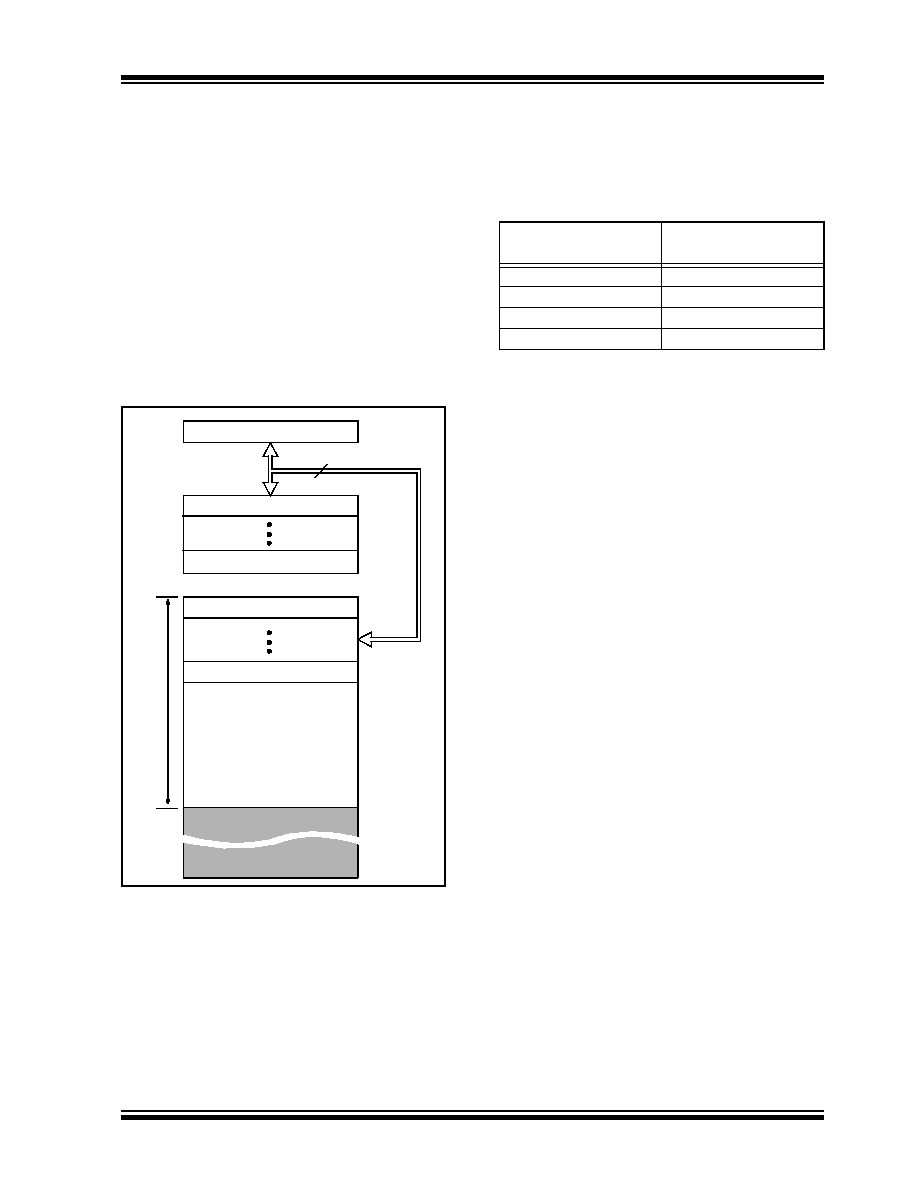
FIGURE 2-1:
PROGRAM MEMORY MAP
AND STACK OF MCV18E
2.2
Data Memory Organization
The data memory is partitioned into multiple banks
which contain the General Purpose Registers (GPR)
and the Special Function Registers (SFR). Bits RP1
and RP0 of the STATUS register are the bank select
bits.
Each bank extends up to 7Fh (128 bytes). The lower
locations of each bank are reserved for the Special
Function Registers. Above the Special Function
Registers
are
General
Purpose
Registers,
implemented as static RAM. All implemented banks
contain Special Function Registers. The upper 16 bytes
of GPR space and some “high use” Special Function
Registers in Bank 0 are mirrored in Bank 1 for code
reduction and quicker access.
PC<12:0>
13
0000h
0004h
0005h
07FFh
0800h
1FFFh
Stack Level 1
Stack Level 8
Reset Vector
Interrupt Vector
On-chip Program
Memory
CALL, RETURN
RETFIE, RETLW
U
s
e
rMe
mo
ry
Sp
a
c
e
RP<1:0>(1)
(Status<6:5>)
Bank
00
0
01
1
10
2(2)
11
3(2)
Note 1:
Maintain Status bit 6 clear to ensure
upward compatibility with future products.
2:
Not implemented
相关PDF资料 |
PDF描述 |
|---|---|
| MD8086-2/B | 16-BIT, 8 MHz, MICROPROCESSOR, CDIP40 |
| MD80C154-12/883D | 8-BIT, 12 MHz, MICROCONTROLLER, CDIP40 |
| MR83C154TXXX-20/883 | 8-BIT, MROM, 20 MHz, MICROCONTROLLER, CQCC44 |
| MR83C154XXX-20/883D | 8-BIT, MROM, 20 MHz, MICROCONTROLLER, CQCC44 |
| MQ83C154XXX-20/883 | 8-BIT, MROM, 20 MHz, MICROCONTROLLER, CQFP44 |
相关代理商/技术参数 |
参数描述 |
|---|---|
| MC-V190H | 制造商:Panasonic Industrial Company 功能描述:FILTER KIT |
| M-CV193H | 制造商:Panasonic Industrial Company 功能描述:OD005 |
| MC-V193H | 制造商:Panasonic Industrial Company 功能描述:FILTER KIT |
| MCV19ES | 制造商:Mencom 功能描述: |
| MCV-19FP-FW | 制造商:Mencom 功能描述: |
发布紧急采购,3分钟左右您将得到回复。