- 您现在的位置:买卖IC网 > PDF目录16593 > MCZ33742SEGR2 (Freescale Semiconductor)IC SYSTEM BASIS CHIP CAN 28-SOIC PDF资料下载
参数资料
| 型号: | MCZ33742SEGR2 |
| 厂商: | Freescale Semiconductor |
| 文件页数: | 32/71页 |
| 文件大小: | 0K |
| 描述: | IC SYSTEM BASIS CHIP CAN 28-SOIC |
| 标准包装: | 1,000 |
| 应用: | 自动 |
| 电流 - 电源: | 42mA |
| 电源电压: | 5.5 V ~ 18 V |
| 工作温度: | -40°C ~ 125°C |
| 安装类型: | 表面贴装 |
| 封装/外壳: | 28-SOIC(0.295",7.50mm 宽) |
| 供应商设备封装: | 28-SOIC W |
| 包装: | 带卷 (TR) |
第1页第2页第3页第4页第5页第6页第7页第8页第9页第10页第11页第12页第13页第14页第15页第16页第17页第18页第19页第20页第21页第22页第23页第24页第25页第26页第27页第28页第29页第30页第31页当前第32页第33页第34页第35页第36页第37页第38页第39页第40页第41页第42页第43页第44页第45页第46页第47页第48页第49页第50页第51页第52页第53页第54页第55页第56页第57页第58页第59页第60页第61页第62页第63页第64页第65页第66页第67页第68页第69页第70页第71页
Analog Integrated Circuit Device Data
38
Freescale Semiconductor
33742
FUNCTIONAL DEVICE OPERATION
OPERATIONAL MODES
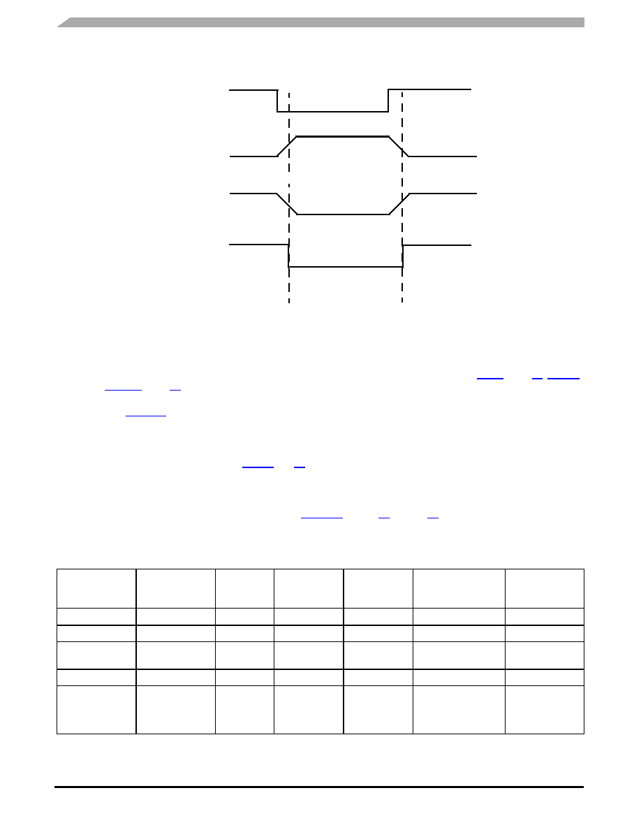
Figure 20. CAN Interface Levels
TXD AND RXD PINS
The TXD pin has an internal pull-up to V2. The state of TXD depends on the V2 status. RXD is a push-pull structure, supplied
by V2. When V2 is set at 5.0 V and CAN is TXRX mode, RXD reports bus status. For details, refer to Table , page 28, Table 9,
The TXD pin is a push-pull structure between the V2 pin and GND. The circuitry has a parasitic diode between RXD and V2.
It is illustrated in Figure 25. This parasitic diode is reversed biased in normal operation (TXD voltage is lower or equal to V2). In
case the TXD voltage is greater than V2, a current will flow into the diode.
If the V2 pin is low (e.g. in sleep mode, or in stop with a ballast transistor), the current leakage at V2 is low enough (10
A
max) to ensure than the RXD pin can be pulled up by an external resistor (i.e. the MCU RXD pin internal pull-up).
The states of the RXD pin in the following Table 9 and 10 is dependant upon external circuitry connected to the V2 and RXD
pins.
CAN TXRX MODE AND SLEW RATE SELECTION
The slew rate selection is done via CAN register (refer to Tables 22 through 24 on page 50). Four slew rates are available and
control the recessive-to-dominant and dominant-to-recessive transitions. The delay time from TXD pin to CAN bus, from CAN
bus to RXD, and from the TXD to RXD loop time is affected by the slew rate selection.
Table 9. CAN Interface/33742S Modes and Pin Status—Operation with Ballast on V2(45)
Mode
CAN Mode
(Controlled by SPI)
V2 Voltage
TXD Pin
RXD Pin(46)
CANH/CANL
(Disconnected from
Other Node)
CAN
Communication
Unpowered
–
0.0 V
LOW
Floating to GND
NO
Reset (with Ballast)
–
0.0 V
LOW
Floating to GND
NO
Normal Request
(with Ballast)
–
0.0 V
LOW
Floating to GND
NO
Normal
Sleep
5.0 V
0.0 V
5.0 V
Floating to GND
NO
Normal
Slew Rate 0, 1, 2, 3
5.0 V
Internal Pull-up
to V2
Report Bus State
HIGH if Bus
Recessive,
LOW if dominant
Bus Recessive
CANH = CANL = 2.5 V
YES
CANH
TXD
RXD
Typ 2.5 V
CANL
CAN Recessive State
CAN Dominant State
CAN Recessive State
Typ 2.5 V
VCANH-VCANL > 900 mV
VCANH-VCANL < 500 mV
相关PDF资料 |
PDF描述 |
|---|---|
| H3AKH-3418G | IDC CABLE - HSC34H/AE34G/HPK34H |
| EVAL-AD5235SDZ | BOARD EVAL FOR AD5235 |
| MCZ33742EGR2 | IC SYSTEM BASIS CHIP CAN 28-SOIC |
| ECM30DCAN | CONN EDGECARD 60POS R/A .156 SLD |
| EVAL-ADCMP561BRQZ | BOARD EVALUATION ADCMP561BRQZ |
相关代理商/技术参数 |
参数描述 |
|---|---|
| MCZ33780EG | 功能描述:多路器开关 IC DBUS MASTER RoHS:否 制造商:Texas Instruments 通道数量:1 开关数量:4 开启电阻(最大值):7 Ohms 开启时间(最大值): 关闭时间(最大值): 传播延迟时间:0.25 ns 工作电源电压:2.3 V to 3.6 V 工作电源电流: 最大工作温度:+ 85 C 安装风格:SMD/SMT 封装 / 箱体:UQFN-16 |
| MCZ33780EG | 制造商:Freescale Semiconductor 功能描述:DUAL DBUS MASTER INTERFACE 16SOIC |
| MCZ33780EGR2 | 功能描述:多路器开关 IC DBUS MASTER RoHS:否 制造商:Texas Instruments 通道数量:1 开关数量:4 开启电阻(最大值):7 Ohms 开启时间(最大值): 关闭时间(最大值): 传播延迟时间:0.25 ns 工作电源电压:2.3 V to 3.6 V 工作电源电流: 最大工作温度:+ 85 C 安装风格:SMD/SMT 封装 / 箱体:UQFN-16 |
| MCZ33781EK | 功能描述:输入/输出控制器接口集成电路 DBUS2 MASTER STND RoHS:否 制造商:Silicon Labs 产品: 输入/输出端数量: 工作电源电压: 最大工作温度:+ 85 C 最小工作温度:- 40 C 安装风格:SMD/SMT 封装 / 箱体:QFN-64 封装:Tray |
| MCZ33781EKR2 | 功能描述:输入/输出控制器接口集成电路 DBUS2 MASTER STND RoHS:否 制造商:Silicon Labs 产品: 输入/输出端数量: 工作电源电压: 最大工作温度:+ 85 C 最小工作温度:- 40 C 安装风格:SMD/SMT 封装 / 箱体:QFN-64 封装:Tray |
发布紧急采购,3分钟左右您将得到回复。