- 您现在的位置:买卖IC网 > PDF目录95978 > MMDF6N02HDR2 (ON SEMICONDUCTOR) 6500 mA, 20 V, N-CHANNEL, Si, SMALL SIGNAL, MOSFET PDF资料下载
参数资料
| 型号: | MMDF6N02HDR2 |
| 厂商: | ON SEMICONDUCTOR |
| 元件分类: | 小信号晶体管 |
| 英文描述: | 6500 mA, 20 V, N-CHANNEL, Si, SMALL SIGNAL, MOSFET |
| 封装: | MINIATURE, CASE 751-07, SOP-8 |
| 文件页数: | 7/10页 |
| 文件大小: | 227K |
| 代理商: | MMDF6N02HDR2 |
MMDF6N02HD
http://onsemi.com
6
I S
,SOURCE
CURRENT
t, TIME
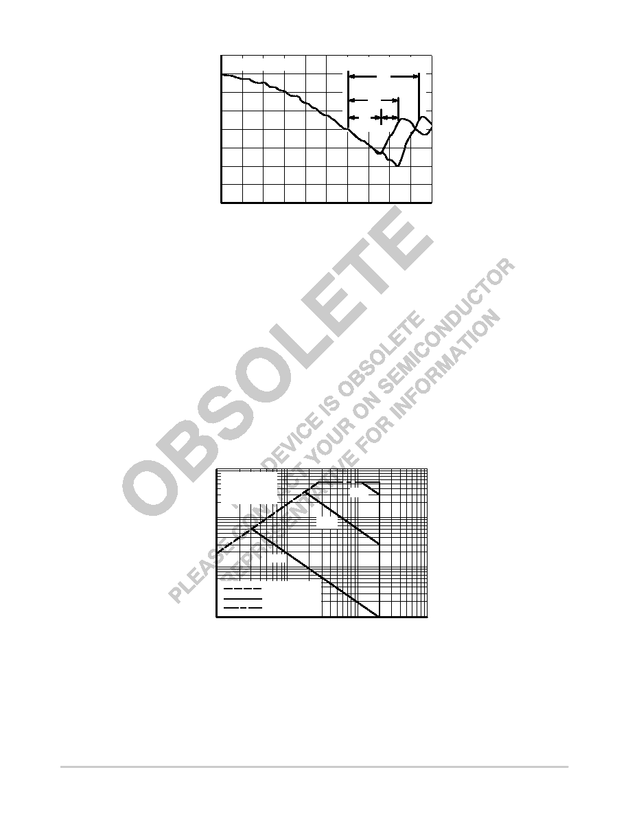
Figure 11. Reverse Recovery Time (trr)
di/dt = 300 A/
μs
Standard Cell Density
High Cell Density
tb
trr
ta
trr
SAFE OPERATING AREA
The Forward Biased Safe Operating Area curves define
the maximum simultaneous draintosource voltage and
drain current that a transistor can handle safely when it is
forward biased. Curves are based upon maximum peak
junction temperature and a case temperature (TC) of 25°C.
Peak repetitive pulsed power limits are determined by using
the thermal response data in conjunction with the procedures
discussed in AN569, “Transient Thermal Resistance
General Data and Its Use.”
Switching between the offstate and the onstate may
traverse any load line provided neither rated peak current
(IDM) nor rated voltage (VDSS) is exceeded, and that the
transition time (tr, tf) does not exceed 10 μs. In addition the
total power averaged over a complete switching cycle must
not exceed (TJ(MAX) TC)/(RθJC).
A power MOSFET designated EFET can be safely used
in switching circuits with unclamped inductive loads. For
reliable operation, the stored energy from circuit inductance
dissipated in the transistor while in avalanche must be less
than the rated limit and must be adjusted for operating
conditions differing from those specified. Although industry
practice is to rate in terms of energy, avalanche energy
capability is not a constant. The energy rating decreases
nonlinearly with an increase of peak current in avalanche
and peak junction temperature.
Figure 12. Maximum Rated Forward Biased
Safe Operating Area
0.1
VDS, DRAINTOSOURCE VOLTAGE (VOLTS)
1
10
I D
,DRAIN
CURRENT
(AMPS)
RDS(on) LIMIT
THERMAL LIMIT
PACKAGE LIMIT
VGS = 12 V
SINGLE PULSE
TC = 25°C
10
0.1
dc
10 ms
1
100
1 ms
相关PDF资料 |
PDF描述 |
|---|---|
| MMDF6N03HDR2 | 6000 mA, 30 V, 2 CHANNEL, N-CHANNEL, Si, SMALL SIGNAL, MOSFET |
| MMDF7N02ZR2 | 7000 mA, 20 V, 2 CHANNEL, N-CHANNEL, Si, SMALL SIGNAL, MOSFET |
| MMDJ3N03BJTR2 | 3 A, 30 V, 2 CHANNEL, NPN, Si, POWER TRANSISTOR |
| MMDJ3N03BJT | 3 A, 30 V, 2 CHANNEL, NPN, Si, POWER TRANSISTOR |
| MMDJ3P03BJTR2 | 3 A, 30 V, 2 CHANNEL, PNP, Si, POWER TRANSISTOR |
相关代理商/技术参数 |
参数描述 |
|---|---|
| MMDF6N03HD | 制造商:MOTOROLA 制造商全称:Motorola, Inc 功能描述:DUAL TMOS POWER MOSFET 30 VOLTS |
| MMDF6N03HDR2 | 制造商:ONSEMI 制造商全称:ON Semiconductor 功能描述:Power MOSFET 6 Amps, 30 Volts |
| MMDF7N02Z | 制造商:MOTOROLA 制造商全称:Motorola, Inc 功能描述:DUAL TMOS POWER MOSFET 7.0 AMPERES 20 VOLTS |
| MMDF7N02ZR2 | 制造商:ON Semiconductor 功能描述:Trans MOSFET N-CH 20V 7A 8-Pin SOIC N T/R 制造商:Rochester Electronics LLC 功能描述:- Bulk |
| MMDFS2P102 | 制造商:MOTOROLA 制造商全称:Motorola, Inc 功能描述:P-Channel Power MOSFET with Schottky Rectifier 20 Volts |
发布紧急采购,3分钟左右您将得到回复。