- 您现在的位置:买卖IC网 > PDF目录95978 > MMDF6N03HDR2 (MOTOROLA INC) 6000 mA, 30 V, 2 CHANNEL, N-CHANNEL, Si, SMALL SIGNAL, MOSFET PDF资料下载
参数资料
| 型号: | MMDF6N03HDR2 |
| 厂商: | MOTOROLA INC |
| 元件分类: | 小信号晶体管 |
| 英文描述: | 6000 mA, 30 V, 2 CHANNEL, N-CHANNEL, Si, SMALL SIGNAL, MOSFET |
| 文件页数: | 7/10页 |
| 文件大小: | 207K |
| 代理商: | MMDF6N03HDR2 |
MMDF6N03HD
6
Motorola TMOS Power MOSFET Transistor Device Data
I S
,SOURCE
CURRENT
t, TIME
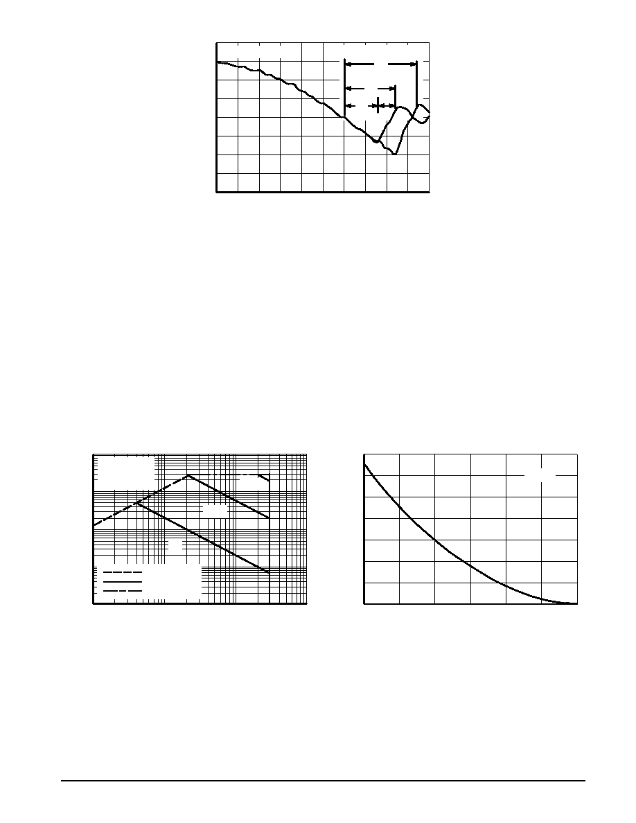
Figure 11. Reverse Recovery Time (trr)
di/dt = 300 A/
s
Standard Cell Density
High Cell Density
tb
trr
ta
trr
SAFE OPERATING AREA
The Forward Biased Safe Operating Area curves define
the maximum simultaneous drain–to–source voltage and
drain current that a transistor can handle safely when it is for-
ward biased. Curves are based upon maximum peak junc-
tion temperature and a case temperature (TC) of 25°C. Peak
repetitive pulsed power limits are determined by using the
thermal response data in conjunction with the procedures
discussed in AN569, “Transient Thermal Resistance – Gen-
eral Data and Its Use.”
Switching between the off–state and the on–state may tra-
verse any load line provided neither rated peak current (IDM)
nor rated voltage (VDSS) is exceeded, and that the transition
time (tr, tf) does not exceed 10 s. In addition the total power
averaged over a complete switching cycle must not exceed
(TJ(MAX) – TC)/(R
θJC).
A power MOSFET designated E–FET can be safely used
in switching circuits with unclamped inductive loads. For reli-
able operation, the stored energy from circuit inductance dis-
sipated in the transistor while in avalanche must be less than
the rated limit and must be adjusted for operating conditions
differing from those specified. Although industry practice is to
rate in terms of energy, avalanche energy capability is not a
constant. The energy rating decreases non–linearly with an
increase of peak current in avalanche and peak junction tem-
perature.
Figure 12. Maximum Rated Forward Biased
Safe Operating Area
0.1
VDS, DRAIN–TO–SOURCE VOLTAGE (VOLTS)
1.0
10
I D
,DRAIN
CURRENT
(AMPS)
RDS(on) LIMIT
THERMAL LIMIT
PACKAGE LIMIT
VGS = 12 V
SINGLE PULSE
TA = 25°C
10
0.01
dc
10 ms
1.0
100
1.0 ms
0.1
Figure 13. Maximum Avalanche Energy versus
Starting Junction Temperature
25
TJ, STARTING JUNCTION TEMPERATURE (°C)
250
300
E
AS
,SINGLE
PULSE
DRAIN–T
O–SOURCE
65
0
45
350
145
50
85
125
105
A
V
ALANCHE
ENERGY
(mJ)
100
150
200
ID = 6 A
相关PDF资料 |
PDF描述 |
|---|---|
| MMDF7N02ZR2 | 7000 mA, 20 V, 2 CHANNEL, N-CHANNEL, Si, SMALL SIGNAL, MOSFET |
| MMDJ3N03BJTR2 | 3 A, 30 V, 2 CHANNEL, NPN, Si, POWER TRANSISTOR |
| MMDJ3N03BJT | 3 A, 30 V, 2 CHANNEL, NPN, Si, POWER TRANSISTOR |
| MMDJ3P03BJTR2 | 3 A, 30 V, 2 CHANNEL, PNP, Si, POWER TRANSISTOR |
| MMDJ3P03BJT | 3 A, 30 V, 2 CHANNEL, PNP, Si, POWER TRANSISTOR |
相关代理商/技术参数 |
参数描述 |
|---|---|
| MMDF7N02Z | 制造商:MOTOROLA 制造商全称:Motorola, Inc 功能描述:DUAL TMOS POWER MOSFET 7.0 AMPERES 20 VOLTS |
| MMDF7N02ZR2 | 制造商:ON Semiconductor 功能描述:Trans MOSFET N-CH 20V 7A 8-Pin SOIC N T/R 制造商:Rochester Electronics LLC 功能描述:- Bulk |
| MMDFS2P102 | 制造商:MOTOROLA 制造商全称:Motorola, Inc 功能描述:P-Channel Power MOSFET with Schottky Rectifier 20 Volts |
| MMDFS2P102R2 | 制造商:Rochester Electronics LLC 功能描述:- Bulk 制造商:ON Semiconductor 功能描述: |
| MMDFS3P303 | 制造商:ONSEMI 制造商全称:ON Semiconductor 功能描述:Power MOSFET 3 Amps, 30 Volts |
发布紧急采购,3分钟左右您将得到回复。