- 您现在的位置:买卖IC网 > PDF目录95979 > MMFT2955ET1G (ON SEMICONDUCTOR) 1200 mA, 60 V, P-CHANNEL, Si, SMALL SIGNAL, MOSFET, TO-261AA PDF资料下载
参数资料
| 型号: | MMFT2955ET1G |
| 厂商: | ON SEMICONDUCTOR |
| 元件分类: | 小信号晶体管 |
| 英文描述: | 1200 mA, 60 V, P-CHANNEL, Si, SMALL SIGNAL, MOSFET, TO-261AA |
| 封装: | LEAD FREE, CASE 318E-04, 4 PIN |
| 文件页数: | 3/6页 |
| 文件大小: | 203K |
| 代理商: | MMFT2955ET1G |
MMFT2955E
http://onsemi.com
3
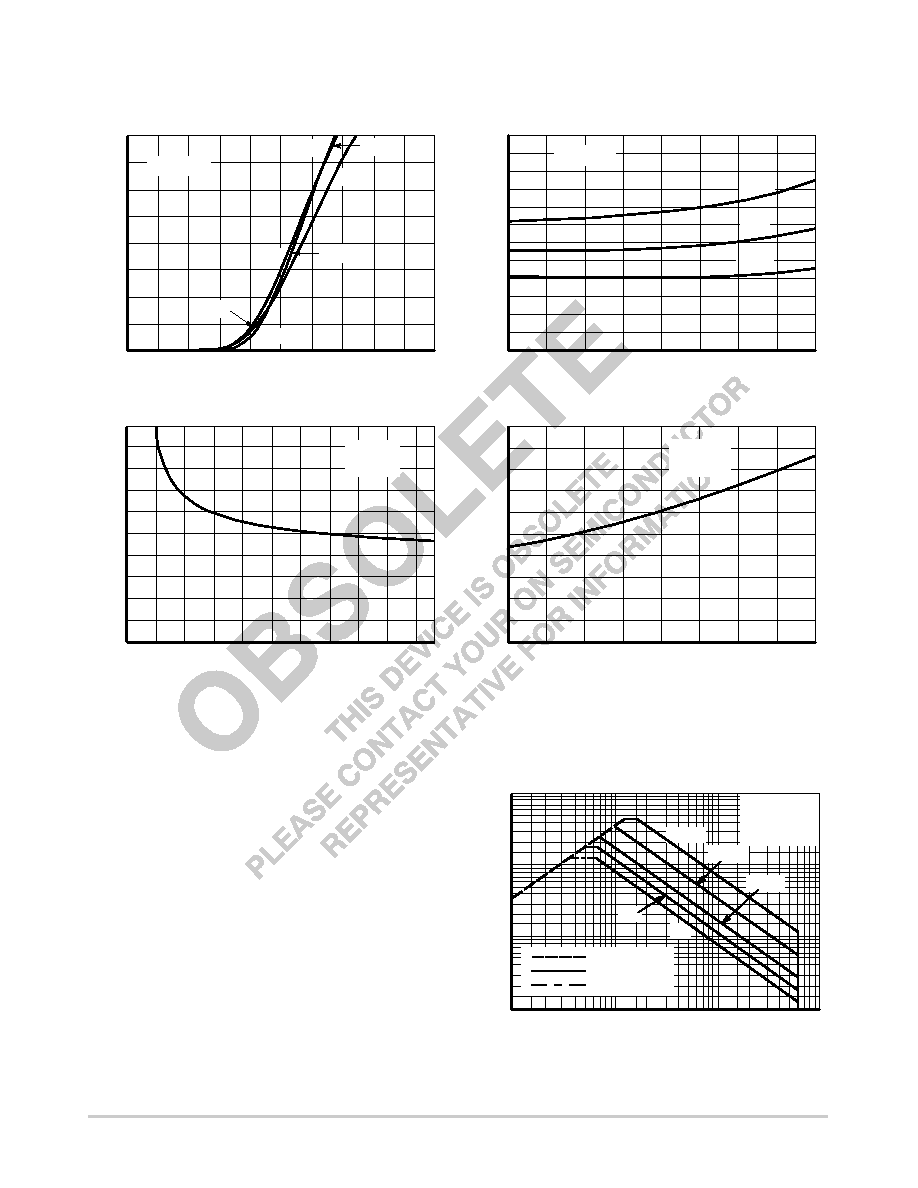
TYPICAL ELECTRICAL CHARACTERISTICS
R
DS(on)
,DRAINT
OSOURCE
RESIST
ANCE
(OHM
S
R
DS(on)
,DRAINT
OSOURCE
RESIST
ANCE
(OHMS)
R
DS(on)
,DRAINT
OSOURCE
RESIST
ANCE
(OHMS)
Figure 3. Transfer Characteristics
Figure 4. OnResistance versus Drain Current
Figure 5. OnResistance versus
GatetoSource Voltage
Figure 6. OnResistance versus
Junction Temperature
8
VGS, GATETOSOURCE VOLTAGE (VOLTS)
I D
,DRAIN
CURRENT
(AMPS)
6
4
2
0
10
8
6
4
2
0
VDS = 10 V
55
°C
25
°C
100
°C
55
°C
25
°C
100
°C
55
°C
ID, DRAIN CURRENT (AMPS)
0.6
0
0.5
0.4
0.3
0.2
0.1
0
24
6
8
VGS = 10 V
100
°C
25
°C
55
°C
0.5
VGS, GATETOSOURCE VOLTAGE (VOLTS)
4
0.4
0.2
0.1
0
0.3
710
13
16
19
TJ = 25°C
ID = 1.2 A
0.5
TJ, JUNCTION TEMPERATURE (°C)
0.4
0.2
0.1
0
0.3
50
0
50
100
150
VGS = 10 V
ID = 1.2 A
FORWARD BIASED SAFE OPERATING AREA
The FBSOA curves define the maximum draintosource
voltage and drain current that a device can safely handle
when it is forward biased, or when it is on, or being turned
on. Because these curves include the limitations of
simultaneous high voltage and high current, up to the rating
of the device, they are especially useful to designers of linear
systems. The curves are based on a ambient temperature of
25°C and a maximum junction temperature of 150°C.
Limitations for repetitive pulses at various ambient
temperatures can be determined by using the thermal
response curves. ON Semiconductor Application Note,
AN569, “Transient Thermal ResistanceGeneral Data and
Its Use” provides detailed instructions.
SWITCHING SAFE OPERATING AREA
The switching safe operating area (SOA) is the boundary
that the load line may traverse without incurring damage to
the MOSFET. The fundamental limits are the peak current,
IDM and the breakdown voltage, BVDSS. The switching
SOA is applicable for both turnon and turnoff of the
devices for switching times less than one microsecond.
Figure 7. Maximum Rated Forward Biased
Safe Operating Area
DI
,DRAIN
CURRENT
(AMPS)
1
0.1
0.01
0.1
10
100
VDS, DRAINTOSOURCE VOLTAGE (VOLTS)
10
1 s
DC
500 ms
1
RDS(on) LIMIT
THERMAL LIMIT
PACKAGE LIMIT
100 ms
20ms
VGS = 20 V
SINGLE PULSE
TA = 25°C
相关PDF资料 |
PDF描述 |
|---|---|
| MMFT2N25EG | 2000 mA, 250 V, N-CHANNEL, Si, SMALL SIGNAL, MOSFET, TO-261AA |
| MMFT3055ET1 | 1700 mA, 60 V, N-CHANNEL, Si, SMALL SIGNAL, MOSFET, TO-261AA |
| MMFT3055ET3 | 1700 mA, 60 V, N-CHANNEL, Si, SMALL SIGNAL, MOSFET |
| MMFT3055ET1 | 1700 mA, 60 V, N-CHANNEL, Si, SMALL SIGNAL, MOSFET |
| MMFT3055ELT3 | 1500 mA, 60 V, N-CHANNEL, Si, SMALL SIGNAL, MOSFET, TO-261AA |
相关代理商/技术参数 |
参数描述 |
|---|---|
| MMFT2N02EL | 制造商:MOTOROLA 制造商全称:Motorola, Inc 功能描述:MEDIUM POWER LOGIC LEVEL TMOS FET 1.6 AMP 20 VOLTS |
| MMFT2N02ELT1 | 功能描述:MOSFET N-CH 20V 1.6A SOT223 RoHS:否 类别:分离式半导体产品 >> FET - 单 系列:- 标准包装:1,000 系列:MESH OVERLAY™ FET 型:MOSFET N 通道,金属氧化物 FET 特点:逻辑电平门 漏极至源极电压(Vdss):200V 电流 - 连续漏极(Id) @ 25° C:18A 开态Rds(最大)@ Id, Vgs @ 25° C:180 毫欧 @ 9A,10V Id 时的 Vgs(th)(最大):4V @ 250µA 闸电荷(Qg) @ Vgs:72nC @ 10V 输入电容 (Ciss) @ Vds:1560pF @ 25V 功率 - 最大:40W 安装类型:通孔 封装/外壳:TO-220-3 整包 供应商设备封装:TO-220FP 包装:管件 |
| MMFT2N25E | 制造商:MOTOROLA 制造商全称:Motorola, Inc 功能描述:TMOS POWER FET 2.0 AMPERES 250 VOLTS |
| MMFT2N25ET3 | 制造商:Rochester Electronics LLC 功能描述:- Tape and Reel |
| MMFT3055E | 制造商:MOTOROLA 制造商全称:Motorola, Inc 功能描述:MEDIUM POWER TMOS FET 1.7 AMP 60 VOLTS |
发布紧急采购,3分钟左右您将得到回复。