- 您现在的位置:买卖IC网 > PDF目录95979 > MMFT3055VLT1G (ON SEMICONDUCTOR) 1500 mA, 60 V, N-CHANNEL, Si, SMALL SIGNAL, MOSFET, TO-261AA PDF资料下载
参数资料
| 型号: | MMFT3055VLT1G |
| 厂商: | ON SEMICONDUCTOR |
| 元件分类: | 小信号晶体管 |
| 英文描述: | 1500 mA, 60 V, N-CHANNEL, Si, SMALL SIGNAL, MOSFET, TO-261AA |
| 封装: | CASE 318E-04, 4 PIN |
| 文件页数: | 9/10页 |
| 文件大小: | 219K |
| 代理商: | MMFT3055VLT1G |
MMFT3055VL
http://onsemi.com
8
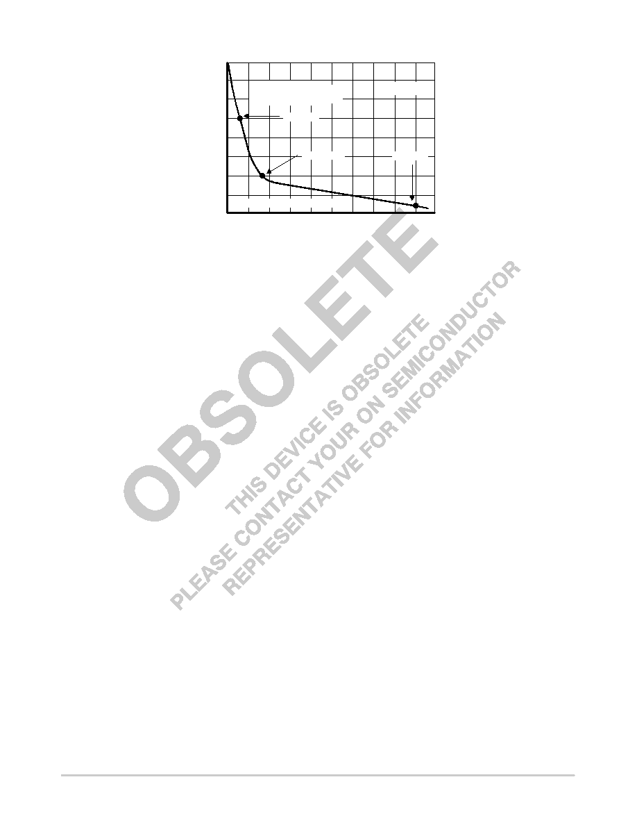
0.8 Watts
1.25 Watts*
1.5 Watts
A, Area (square inches)
0.0
0.2
0.4
0.6
0.8
1.0
160
140
120
100
80
Figure 15. Thermal Resistance versus Drain Pad
Area for the SOT223 Package (Typical)
Board Material = 0.0625″
G10/FR4, 2 oz Copper
TA = 25°C
*Mounted on the DPAK footprint
R
,
Thermal
Resistance,
Junction
to
Ambient
(C/W)
θ JA
°
Another alternative would be to use a ceramic substrate
or an aluminum core board such as Thermal Clad
t. Using
a board material such as Thermal Clad, an aluminum core
board, the power dissipation can be doubled using the same
footprint.
SOLDER STENCIL GUIDELINES
Prior to placing surface mount components onto a printed
circuit board, solder paste must be applied to the pads. A
solder stencil is required to screen the optimum amount of
solder paste onto the footprint. The stencil is made of brass
or stainless steel with a typical thickness of 0.008 inches.
The stencil opening size for the SOT223 package should
be the same as the pad size on the printed circuit board, i.e.,
a 1:1 registration.
SOLDERING PRECAUTIONS
The melting temperature of solder is higher than the rated
temperature of the device. When the entire device is heated
to a high temperature, failure to complete soldering within
a short time could result in device failure. Therefore, the
following items should always be observed in order to
minimize the thermal stress to which the devices are
subjected.
Always preheat the device.
The delta temperature between the preheat and
soldering should be 100°C or less.*
When preheating and soldering, the temperature of the
leads and the case must not exceed the maximum
temperature ratings as shown on the data sheet. When
using infrared heating with the reflow soldering
method, the difference shall be a maximum of 10°C.
The soldering temperature and time shall not exceed
260°C for more than 10 seconds.
When shifting from preheating to soldering, the
maximum temperature gradient shall be 5°C or less.
After soldering has been completed, the device should
be allowed to cool naturally for at least three minutes.
Gradual cooling should be used as the use of forced
cooling will increase the temperature gradient and
result in latent failure due to mechanical stress.
Mechanical stress or shock should not be applied
during cooling
* * Soldering a device without preheating can cause
excessive thermal shock and stress which can result in
damage to the device.
相关PDF资料 |
PDF描述 |
|---|---|
| MMFT3055VLT3G | 1500 mA, 60 V, N-CHANNEL, Si, SMALL SIGNAL, MOSFET, TO-261AA |
| MMFT3055VLT3 | 1500 mA, 60 V, N-CHANNEL, Si, SMALL SIGNAL, MOSFET, TO-261AA |
| MMFT3055VLT1 | 1500 mA, 60 V, N-CHANNEL, Si, SMALL SIGNAL, MOSFET, TO-261AA |
| MMFT3055VLT3 | 1500 mA, 60 V, N-CHANNEL, Si, SMALL SIGNAL, MOSFET, TO-261AA |
| MMFT3055VLT1 | 1500 mA, 60 V, N-CHANNEL, Si, SMALL SIGNAL, MOSFET, TO-261AA |
相关代理商/技术参数 |
参数描述 |
|---|---|
| MMFT3055VT1 | 制造商:ON Semiconductor 功能描述:Trans MOSFET N-CH 60V 1.7A 4-Pin(3+Tab) SOT-223 T/R |
| MMFT3055VT3 | 制造商:ON Semiconductor 功能描述:Trans MOSFET N-CH 60V 1.7A 4-Pin(3+Tab) SOT-223 T/R |
| MMFT5P03HD | 制造商:MOTOROLA 制造商全称:Motorola, Inc 功能描述:TMOS MEDIUM POWER FET 5.2 AMPERES 30 VOLTS |
| MMFT5P03HDT1 | 功能描述:MOSFET P-CH 30V 3.7A SOT223 RoHS:否 类别:分离式半导体产品 >> FET - 单 系列:- 标准包装:1,000 系列:MESH OVERLAY™ FET 型:MOSFET N 通道,金属氧化物 FET 特点:逻辑电平门 漏极至源极电压(Vdss):200V 电流 - 连续漏极(Id) @ 25° C:18A 开态Rds(最大)@ Id, Vgs @ 25° C:180 毫欧 @ 9A,10V Id 时的 Vgs(th)(最大):4V @ 250µA 闸电荷(Qg) @ Vgs:72nC @ 10V 输入电容 (Ciss) @ Vds:1560pF @ 25V 功率 - 最大:40W 安装类型:通孔 封装/外壳:TO-220-3 整包 供应商设备封装:TO-220FP 包装:管件 |
| MMFT5P03HDT3 | 制造商:MOTOROLA 制造商全称:Motorola, Inc 功能描述:TMOS P-CHANNEL FIELD FEECT TRANSISTOR |
发布紧急采购,3分钟左右您将得到回复。