- 您现在的位置:买卖IC网 > PDF目录80445 > MPC755BRX350LE (FREESCALE SEMICONDUCTOR INC) 32-BIT, 350 MHz, RISC PROCESSOR, CBGA360 PDF资料下载
参数资料
| 型号: | MPC755BRX350LE |
| 厂商: | FREESCALE SEMICONDUCTOR INC |
| 元件分类: | 微控制器/微处理器 |
| 英文描述: | 32-BIT, 350 MHz, RISC PROCESSOR, CBGA360 |
| 封装: | 25 X 25 MM, 3.20 MM HEIGHT, 1.27 MM PITCH, CERAMIC, BGA-360 |
| 文件页数: | 8/60页 |
| 文件大小: | 1559K |
| 代理商: | MPC755BRX350LE |
第1页第2页第3页第4页第5页第6页第7页当前第8页第9页第10页第11页第12页第13页第14页第15页第16页第17页第18页第19页第20页第21页第22页第23页第24页第25页第26页第27页第28页第29页第30页第31页第32页第33页第34页第35页第36页第37页第38页第39页第40页第41页第42页第43页第44页第45页第46页第47页第48页第49页第50页第51页第52页第53页第54页第55页第56页第57页第58页第59页第60页
MPC755 RISC Microprocessor Hardware Specifications, Rev. 7.0
16
Freescale Semiconductor
Electrical and Thermal Characteristics
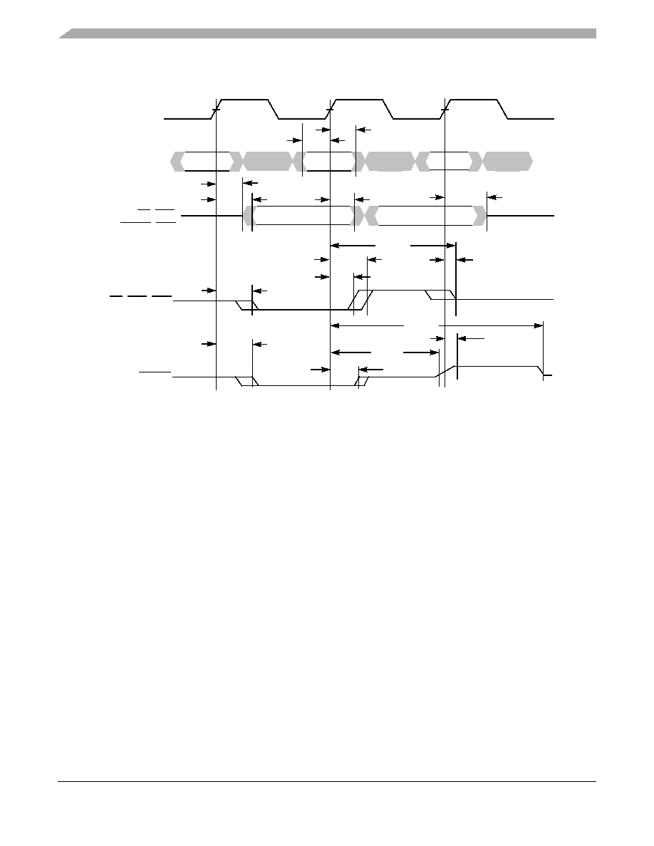
Figure 6 provides the input/output timing diagram for the MPC755.
Figure 6. Input/Output Timing Diagram
4.2.3
L2 Clock AC Specifications
The L2CLK frequency is programmed by the L2 configuration register (L2CR[4–6]) core-to-L2 divisor
ratio. See Table 17 for example core and L2 frequencies at various divisors. Table 11 provides the potential
range of L2CLK output AC timing specifications as defined in Figure 7.
The minimum L2CLK frequency of Table 11 is specified by the maximum delay of the internal DLL. The
variable-tap DLL introduces up to a full clock period delay in the L2CLK_OUTA, L2CLK_OUTB, and
L2SYNC_OUT signals so that the returning L2SYNC_IN signal is phase-aligned with the next core clock
(divided by the L2 divisor ratio). Do not choose a core-to-L2 divisor which results in an L2 frequency
below this minimum, or the L2CLK_OUT signals provided for SRAM clocking will not be phase-aligned
with the MPC755 core clock at the SRAMs.
The maximum L2CLK frequency shown in Table 11 is the core frequency divided by one. Very few L2
SRAM designs will be able to operate in this mode, especially at higher core frequencies. Therefore, most
designs will select a greater core-to-L2 divisor to provide a longer L2CLK period for read and write access
to the L2 SRAMs. The maximum L2CLK frequency for any application of the MPC755 will be a function
of the AC timings of the MPC755, the AC timings for the SRAM, bus loading, and printed-circuit board
trace length. The current AC timing of the MPC755 supports up to 200 MHz with typical, similarly-rated
SRAM parts, provided careful design practices are observed. Clock trace lengths must be matched and all
trace lengths should be as short as possible. Higher frequencies can be achieved by using better performing
SYSCLK
All Inputs
VM
All Outputs
tKHOX
VM
(Except TS, ABB,
ARTRY, DBB)
TS, ABB, DBB
ARTRY
VM
tKHOZ
tKHABPZ
tKHARPZ
tKHARP
tKHOV
tKHOX
tKHOV
tKHOX
tKHOV
tIVKH
tIXKH
tKHOZ
tKHOE
VM = Midpoint Voltage (OVDD/2 or Vin/2)
相关PDF资料 |
PDF描述 |
|---|---|
| MPC8250AZQIHBC | 32-BIT, 200 MHz, RISC PROCESSOR, PBGA516 |
| MPC859TZP133 | 32-BIT, 133 MHz, RISC PROCESSOR, PBGA357 |
| MC68332GCFV20 | 32-BIT, 20 MHz, MICROCONTROLLER, PQFP144 |
| MC68HC05B16CB | 8-BIT, MROM, 2.1 MHz, MICROCONTROLLER, PDIP56 |
| MC68HC05C8AMFB | 8-BIT, MROM, 2.1 MHz, MICROCONTROLLER, PQFP44 |
相关代理商/技术参数 |
参数描述 |
|---|---|
| MPC755BRX350TE | 功能描述:微处理器 - MPU 360CBGA,RV2.8,HIP4DP RoHS:否 制造商:Atmel 处理器系列:SAMA5D31 核心:ARM Cortex A5 数据总线宽度:32 bit 最大时钟频率:536 MHz 程序存储器大小:32 KB 数据 RAM 大小:128 KB 接口类型:CAN, Ethernet, LIN, SPI,TWI, UART, USB 工作电源电压:1.8 V to 3.3 V 最大工作温度:+ 85 C 安装风格:SMD/SMT 封装 / 箱体:FBGA-324 |
| MPC755BVT300LE | 功能描述:微处理器 - MPU RV2.8106C RoHS:否 制造商:Atmel 处理器系列:SAMA5D31 核心:ARM Cortex A5 数据总线宽度:32 bit 最大时钟频率:536 MHz 程序存储器大小:32 KB 数据 RAM 大小:128 KB 接口类型:CAN, Ethernet, LIN, SPI,TWI, UART, USB 工作电源电压:1.8 V to 3.3 V 最大工作温度:+ 85 C 安装风格:SMD/SMT 封装 / 箱体:FBGA-324 |
| MPC755BVT350LE | 功能描述:微处理器 - MPU RV2.8,106C RoHS:否 制造商:Atmel 处理器系列:SAMA5D31 核心:ARM Cortex A5 数据总线宽度:32 bit 最大时钟频率:536 MHz 程序存储器大小:32 KB 数据 RAM 大小:128 KB 接口类型:CAN, Ethernet, LIN, SPI,TWI, UART, USB 工作电源电压:1.8 V to 3.3 V 最大工作温度:+ 85 C 安装风格:SMD/SMT 封装 / 箱体:FBGA-324 |
| MPC755CPX350LE | 功能描述:微处理器 - MPU 360PBGA,RV2.8,6W RoHS:否 制造商:Atmel 处理器系列:SAMA5D31 核心:ARM Cortex A5 数据总线宽度:32 bit 最大时钟频率:536 MHz 程序存储器大小:32 KB 数据 RAM 大小:128 KB 接口类型:CAN, Ethernet, LIN, SPI,TWI, UART, USB 工作电源电压:1.8 V to 3.3 V 最大工作温度:+ 85 C 安装风格:SMD/SMT 封装 / 箱体:FBGA-324 |
| MPC755CPX400LE | 功能描述:微处理器 - MPU GF RV2.8360PBGA 4A105C RoHS:否 制造商:Atmel 处理器系列:SAMA5D31 核心:ARM Cortex A5 数据总线宽度:32 bit 最大时钟频率:536 MHz 程序存储器大小:32 KB 数据 RAM 大小:128 KB 接口类型:CAN, Ethernet, LIN, SPI,TWI, UART, USB 工作电源电压:1.8 V to 3.3 V 最大工作温度:+ 85 C 安装风格:SMD/SMT 封装 / 箱体:FBGA-324 |
发布紧急采购,3分钟左右您将得到回复。