- 您现在的位置:买卖IC网 > PDF目录80430 > MPC8315VRAGDA (FREESCALE SEMICONDUCTOR INC) 32-BIT, 400 MHz, MICROPROCESSOR, PBGA620 PDF资料下载
参数资料
| 型号: | MPC8315VRAGDA |
| 厂商: | FREESCALE SEMICONDUCTOR INC |
| 元件分类: | 微控制器/微处理器 |
| 英文描述: | 32-BIT, 400 MHz, MICROPROCESSOR, PBGA620 |
| 封装: | 29 X 29 MM, 2.23 MM HEIGHT, 1 MM PITCH, LEAD FREE, TEPBGAII-620 |
| 文件页数: | 11/112页 |
| 文件大小: | 1283K |
| 代理商: | MPC8315VRAGDA |
第1页第2页第3页第4页第5页第6页第7页第8页第9页第10页当前第11页第12页第13页第14页第15页第16页第17页第18页第19页第20页第21页第22页第23页第24页第25页第26页第27页第28页第29页第30页第31页第32页第33页第34页第35页第36页第37页第38页第39页第40页第41页第42页第43页第44页第45页第46页第47页第48页第49页第50页第51页第52页第53页第54页第55页第56页第57页第58页第59页第60页第61页第62页第63页第64页第65页第66页第67页第68页第69页第70页第71页第72页第73页第74页第75页第76页第77页第78页第79页第80页第81页第82页第83页第84页第85页第86页第87页第88页第89页第90页第91页第92页第93页第94页第95页第96页第97页第98页第99页第100页第101页第102页第103页第104页第105页第106页第107页第108页第109页第110页第111页第112页
MPC8315E PowerQUICC II Pro Processor Hardware Specifications, Rev. 0
108
Freescale Semiconductor
System Design Information
26.4
Connection Recommendations
To ensure reliable operation, it is highly recommended to connect unused inputs to an appropriate signal
level. Unused active low inputs should be tied to NVDD, GVDD, or LVDD as required. Unused active
high inputs should be connected to GND. All NC (no-connect) signals must remain unconnected.
Power and ground connections must be made to all external VDD, GVDD, LVDD, NVDD, and GND pins
of the device.
26.5
Output Buffer DC Impedance
The MPC8315E drivers are characterized over process, voltage, and temperature. For all buses, the driver
is a push-pull single-ended driver type (open drain for I2C).
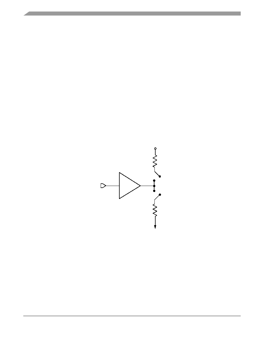
To measure Z0 for the single-ended drivers, an external resistor is connected from the chip pad to NVDD
or GND. Then, the value of each resistor is varied until the pad voltage is NVDD/2 (see Figure 64). The
output impedance is the average of two components, the resistances of the pull-up and pull-down devices.
When data is held high, SW1 is closed (SW2 is open) and RP is trimmed until the voltage at the pad equals
NVDD/2. RP then becomes the resistance of the pull-up devices. RP and RN are designed to be close to
each other in value. Then, Z0 = (RP + RN)/2.
Figure 64. Driver Impedance Measurement
The value of this resistance and the strength of the driver’s current source can be found by making two
measurements. First, the output voltage is measured while driving logic 1 without an external differential
termination resistor. The measured voltage is V1 = Rsource × Isource. Second, the output voltage is measured
while driving logic 1 with an external precision differential termination resistor of value Rterm. The
measured voltage is V2 =(1/(1/R1 +1/R2)) × Isource. Solving for the output impedance gives Rsource =
Rterm × (V1/V2 – 1). The drive current is then Isource =V1/Rsource.
Table 80 summarizes the signal impedance targets. The driver impedance are targeted at minimum VDD,
nominal NVDD, 105
°C.
NVDD
OGND
RP
RN
Pad
Data
SW1
SW2
相关PDF资料 |
PDF描述 |
|---|---|
| MPC8548ECVUAQGB | 32-BIT, 1000 MHz, MICROPROCESSOR, CBGA783 |
| MPC8548EPXATG | 32-BIT, 1200 MHz, MICROPROCESSOR, PBGA783 |
| MC68LK332GCEH16 | 32-BIT, 16 MHz, MICROCONTROLLER, PQFP132 |
| MC908GT16CFBE | 8-BIT, FLASH, 8 MHz, MICROCONTROLLER, PQFP44 |
| MC8641VU1000NE | 32-BIT, 166.66 MHz, MICROPROCESSOR, CBGA1023 |
相关代理商/技术参数 |
参数描述 |
|---|---|
| MPC8321CVRADDC | 功能描述:微处理器 - MPU 8321 NOPB PBGA W/O ENCR RoHS:否 制造商:Atmel 处理器系列:SAMA5D31 核心:ARM Cortex A5 数据总线宽度:32 bit 最大时钟频率:536 MHz 程序存储器大小:32 KB 数据 RAM 大小:128 KB 接口类型:CAN, Ethernet, LIN, SPI,TWI, UART, USB 工作电源电压:1.8 V to 3.3 V 最大工作温度:+ 85 C 安装风格:SMD/SMT 封装 / 箱体:FBGA-324 |
| MPC8321CVRADDC | 制造商:Freescale Semiconductor 功能描述:Embedded Networking Processor |
| MPC8321CVRAFDC | 功能描述:微处理器 - MPU 8321 NOPB PBGA W/O ENCR RoHS:否 制造商:Atmel 处理器系列:SAMA5D31 核心:ARM Cortex A5 数据总线宽度:32 bit 最大时钟频率:536 MHz 程序存储器大小:32 KB 数据 RAM 大小:128 KB 接口类型:CAN, Ethernet, LIN, SPI,TWI, UART, USB 工作电源电压:1.8 V to 3.3 V 最大工作温度:+ 85 C 安装风格:SMD/SMT 封装 / 箱体:FBGA-324 |
| MPC8321CZQADDC | 功能描述:微处理器 - MPU 8321 PBGA W/O ENCR RoHS:否 制造商:Atmel 处理器系列:SAMA5D31 核心:ARM Cortex A5 数据总线宽度:32 bit 最大时钟频率:536 MHz 程序存储器大小:32 KB 数据 RAM 大小:128 KB 接口类型:CAN, Ethernet, LIN, SPI,TWI, UART, USB 工作电源电压:1.8 V to 3.3 V 最大工作温度:+ 85 C 安装风格:SMD/SMT 封装 / 箱体:FBGA-324 |
| MPC8321CZQAFDC | 功能描述:微处理器 - MPU 8321 PBGA W/O ENCR RoHS:否 制造商:Atmel 处理器系列:SAMA5D31 核心:ARM Cortex A5 数据总线宽度:32 bit 最大时钟频率:536 MHz 程序存储器大小:32 KB 数据 RAM 大小:128 KB 接口类型:CAN, Ethernet, LIN, SPI,TWI, UART, USB 工作电源电压:1.8 V to 3.3 V 最大工作温度:+ 85 C 安装风格:SMD/SMT 封装 / 箱体:FBGA-324 |
发布紧急采购,3分钟左右您将得到回复。