- 您现在的位置:买卖IC网 > PDF目录80476 > MPC8349ZUALF (FREESCALE SEMICONDUCTOR INC) 32-BIT, 667 MHz, MICROPROCESSOR, PBGA672 PDF资料下载
参数资料
| 型号: | MPC8349ZUALF |
| 厂商: | FREESCALE SEMICONDUCTOR INC |
| 元件分类: | 微控制器/微处理器 |
| 英文描述: | 32-BIT, 667 MHz, MICROPROCESSOR, PBGA672 |
| 封装: | 35 X 35 MM, 1.46 MM HEIGHT, 1 MM PITCH, TBGA-672 |
| 文件页数: | 19/88页 |
| 文件大小: | 1014K |
| 代理商: | MPC8349ZUALF |
第1页第2页第3页第4页第5页第6页第7页第8页第9页第10页第11页第12页第13页第14页第15页第16页第17页第18页当前第19页第20页第21页第22页第23页第24页第25页第26页第27页第28页第29页第30页第31页第32页第33页第34页第35页第36页第37页第38页第39页第40页第41页第42页第43页第44页第45页第46页第47页第48页第49页第50页第51页第52页第53页第54页第55页第56页第57页第58页第59页第60页第61页第62页第63页第64页第65页第66页第67页第68页第69页第70页第71页第72页第73页第74页第75页第76页第77页第78页第79页第80页第81页第82页第83页第84页第85页第86页第87页第88页
MPC8349E PowerQUICC II Pro Integrated Host Processor Hardware Specifications, Rev. 10
26
Freescale Semiconductor
Ethernet: Three-Speed Ethernet, MII Management
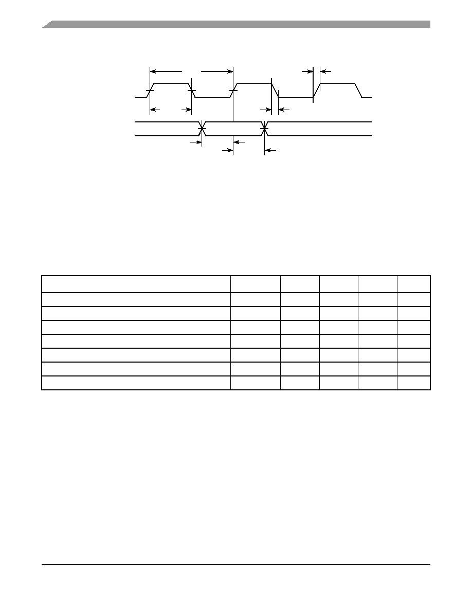
Figure 11 shows the MII receive AC timing diagram.
Figure 11. MII Receive AC Timing Diagram
8.2.3
TBI AC Timing Specifications
This section describes the TBI transmit and receive AC timing specifications.
8.2.3.1
TBI Transmit AC Timing Specifications
Table 25 provides the TBI transmit AC timing specifications.
Table 25. TBI Transmit AC Timing Specifications
At recommended operating conditions with LVDD/OVDD of 3.3 V ± 10%.
Parameter/Condition
Symbol1
Min
Typ
Max
Unit
GTX_CLK clock period
tTTX
—8.0
—
ns
GTX_CLK duty cycle
tTTXH/tTTX
40
—
60
%
GTX_CLK to TBI data TXD[7:0], TX_ER, TX_EN delay
tTTKHDX
1.0
—
5.0
ns
GTX_CLK clock rise, VIL(min) to VIH(max)
tTTXR
——
1.0
ns
GTX_CLK clock fall time, VIH(max) to VIL(min)
tTTXF
——
1.0
ns
GTX_CLK125 reference clock period
tG125
2
—8.0
—
ns
GTX_CLK125 reference clock duty cycle
tG125H/tG125
45
—
55
ns
Notes:
1. The symbols for timing specifications follow the pattern of t(first two letters of functional block)(signal)(state)(reference)(state) for inputs
and t(first two letters of functional block)(reference)(state)(signal)(state) for outputs. For example, tTTKHDV symbolizes the TBI transmit
timing (TT) with respect to the time from tTTX (K) going high (H) until the referenced data signals (D) reach the valid state (V)
or setup time. Also, tTTKHDX symbolizes the TBI transmit timing (TT) with respect to the time from tTTX (K) going high (H) until
the referenced data signals (D) reach the invalid state (X) or hold time. In general, the clock reference symbol is based on
three letters representing the clock of a particular function. For example, the subscript of tTTX represents the TBI (T) transmit
(TX) clock. For rise and fall times, the latter convention is used with the appropriate letter: R (rise) or F (fall).
2. This symbol represents the external GTX_CLK125 and does not follow the original symbol naming convention
RX_CLK
RXD[3:0]
tMRDXKH
tMRX
tMRXH
tMRXR
tMRXF
RX_DV
RX_ER
tMRDVKH
Valid Data
相关PDF资料 |
PDF描述 |
|---|---|
| MPC8343CVRADD | 32-BIT, 266 MHz, RISC PROCESSOR, PBGA620 |
| MC68060RC66 | 32-BIT, 66 MHz, MICROPROCESSOR, CPGA206 |
| MC68LC060FE50 | 32-BIT, 50 MHz, MICROPROCESSOR, CQFP208 |
| MCAQE16G6MPP-MXA | FLASH MEMORY DRIVE CONTROLLER, PQFP |
| MSP430F2416TPM | 16-BIT, FLASH, 16 MHz, RISC MICROCONTROLLER, PQFP64 |
相关代理商/技术参数 |
参数描述 |
|---|---|
| MPC8349ZUALFB | 功能描述:微处理器 - MPU 8349 TBGA W/O ENCRYP RoHS:否 制造商:Atmel 处理器系列:SAMA5D31 核心:ARM Cortex A5 数据总线宽度:32 bit 最大时钟频率:536 MHz 程序存储器大小:32 KB 数据 RAM 大小:128 KB 接口类型:CAN, Ethernet, LIN, SPI,TWI, UART, USB 工作电源电压:1.8 V to 3.3 V 最大工作温度:+ 85 C 安装风格:SMD/SMT 封装 / 箱体:FBGA-324 |
| MPC8358 | 制造商:FREESCALE 制造商全称:Freescale Semiconductor, Inc 功能描述:PowerQUICC⑩ II Pro Processor Revision 2.x TBGA Silicon Hardware Specifications |
| MPC8358CVRADDDA | 功能描述:微处理器 - MPU 8358 PBGA NON-ENC NO-PB RoHS:否 制造商:Atmel 处理器系列:SAMA5D31 核心:ARM Cortex A5 数据总线宽度:32 bit 最大时钟频率:536 MHz 程序存储器大小:32 KB 数据 RAM 大小:128 KB 接口类型:CAN, Ethernet, LIN, SPI,TWI, UART, USB 工作电源电压:1.8 V to 3.3 V 最大工作温度:+ 85 C 安装风格:SMD/SMT 封装 / 箱体:FBGA-324 |
| MPC8358CVRAGDDA | 功能描述:微处理器 - MPU 8358 PBGA NON-ENC NO-PB RoHS:否 制造商:Atmel 处理器系列:SAMA5D31 核心:ARM Cortex A5 数据总线宽度:32 bit 最大时钟频率:536 MHz 程序存储器大小:32 KB 数据 RAM 大小:128 KB 接口类型:CAN, Ethernet, LIN, SPI,TWI, UART, USB 工作电源电压:1.8 V to 3.3 V 最大工作温度:+ 85 C 安装风格:SMD/SMT 封装 / 箱体:FBGA-324 |
| MPC8358CVRAGDGA | 功能描述:微处理器 - MPU 8358 PBGA NON-ENC NO-PB RoHS:否 制造商:Atmel 处理器系列:SAMA5D31 核心:ARM Cortex A5 数据总线宽度:32 bit 最大时钟频率:536 MHz 程序存储器大小:32 KB 数据 RAM 大小:128 KB 接口类型:CAN, Ethernet, LIN, SPI,TWI, UART, USB 工作电源电压:1.8 V to 3.3 V 最大工作温度:+ 85 C 安装风格:SMD/SMT 封装 / 箱体:FBGA-324 |
发布紧急采购,3分钟左右您将得到回复。