- 您现在的位置:买卖IC网 > PDF目录45372 > MPC8569EVTAUNL (FREESCALE SEMICONDUCTOR INC) RISC PROCESSOR, PBGA783 PDF资料下载
参数资料
| 型号: | MPC8569EVTAUNL |
| 厂商: | FREESCALE SEMICONDUCTOR INC |
| 元件分类: | 微控制器/微处理器 |
| 英文描述: | RISC PROCESSOR, PBGA783 |
| 封装: | 29 X 29 MM, 1 MM PITCH, PLASTIC, BGA-783 |
| 文件页数: | 68/126页 |
| 文件大小: | 2847K |
| 代理商: | MPC8569EVTAUNL |
第1页第2页第3页第4页第5页第6页第7页第8页第9页第10页第11页第12页第13页第14页第15页第16页第17页第18页第19页第20页第21页第22页第23页第24页第25页第26页第27页第28页第29页第30页第31页第32页第33页第34页第35页第36页第37页第38页第39页第40页第41页第42页第43页第44页第45页第46页第47页第48页第49页第50页第51页第52页第53页第54页第55页第56页第57页第58页第59页第60页第61页第62页第63页第64页第65页第66页第67页当前第68页第69页第70页第71页第72页第73页第74页第75页第76页第77页第78页第79页第80页第81页第82页第83页第84页第85页第86页第87页第88页第89页第90页第91页第92页第93页第94页第95页第96页第97页第98页第99页第100页第101页第102页第103页第104页第105页第106页第107页第108页第109页第110页第111页第112页第113页第114页第115页第116页第117页第118页第119页第120页第121页第122页第123页第124页第125页第126页
MPC8569E PowerQUICC III Integrated Processor Hardware Specifications, Rev. 0
DDR2 and DDR3 SDRAM Controller
Freescale Semiconductor
46
2.4.1
DDR2 and DDR3 SDRAM Interface DC Electrical Characteristics
The following table provides the recommended operating conditions for the DDR SDRAM controller when interfacing to
DDR2 SDRAM.
The following table provides the recommended operating conditions for the DDR SDRAM controller when interfacing to
DDR3 SDRAM.
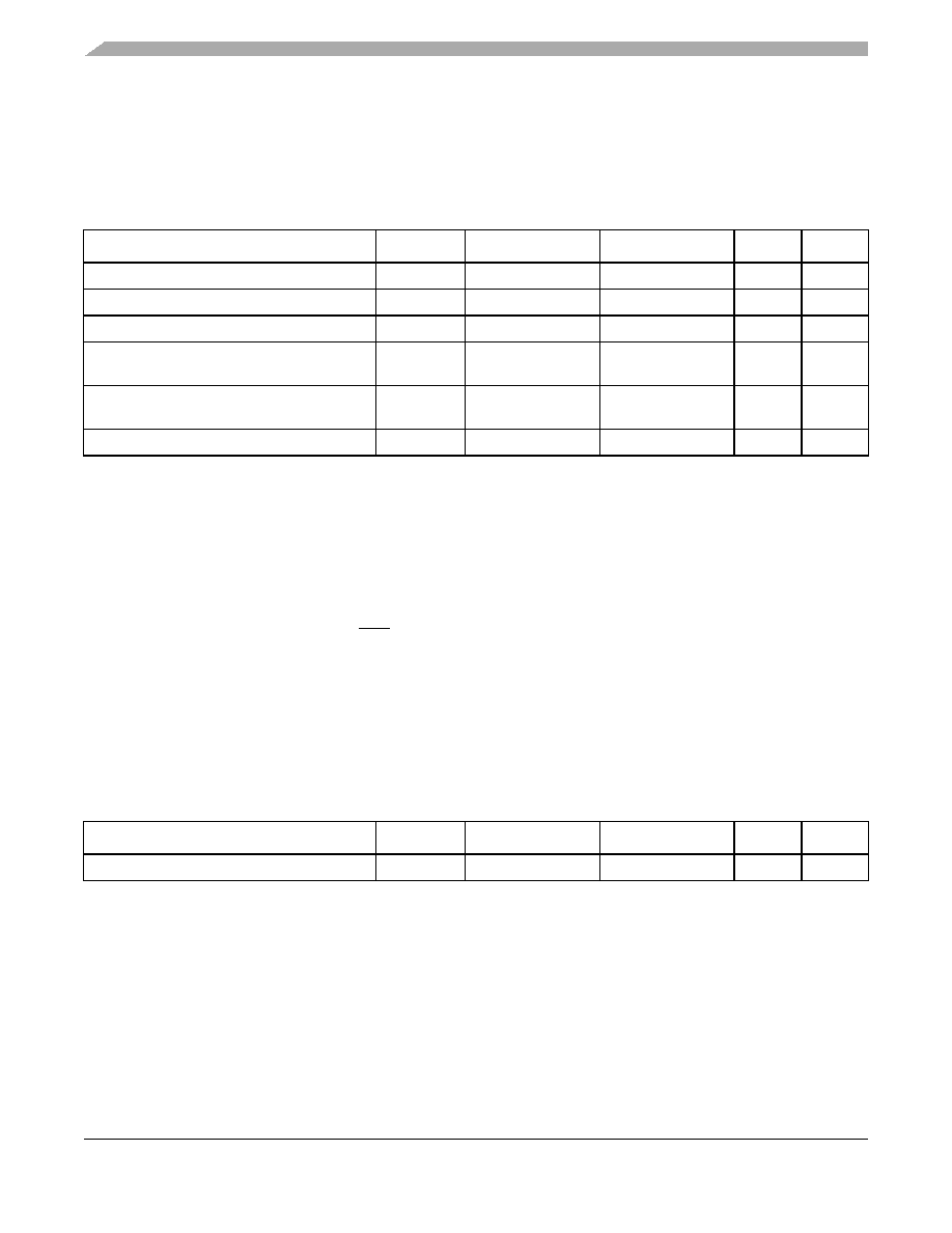
Table 13. DDR2 SDRAM Interface DC Electrical Characteristics
At recommended operating condition with GVDD =1.8 V
1
Parameter
Symbol
Min
Max
Unit
Notes
I/O reference voltage
MVREFn
0.49
× GVDD
0.51
× GVDD
V2, 3, 4
Input high voltage
VIH
MVREFn +0.125
—
V
5
Input low voltage
VIL
—
MVREFn – 0.125
V
5
Output high current (VOUT =1.320 V)
IOH
—–13.4
mA
6, 7
Output low current (VOUT =0.380 V)
IOL
13.4
—
mA
6, 7
I/O leakage current
IOZ
–50
50
μA8
Notes:
1. GVDD is expected to be within 50 mV of the DRAM’s voltage supply at all times. The DRAM’s and memory controller’s voltage
supply may or may not be from the same source.
2. MVREFn is expected to be equal to 0.5
× GVDD and to track GVDD DC variations as measured at the receiver. Peak-to-peak
noise on MVREFn may not exceed the MVREFn DC level by more than ±2% of GVDD (that is, ± 36 mV).
3. VTT is not applied directly to the device. It is the supply to which far end signal termination is made, and it is expected to be
equal to MVREFn with a min value of MVREFn – 0.04 and a max value of MVREFn +0.04. VTT should track variations in the
DC level of MVREFn.
4. The voltage regulator for MVREFn must meet the specifications stated in Table 16.
5. Input capacitance load for DQ, DQS, and DQS are available in the IBIS models.
6. IOH and IOL are measured at GVDD = 1.7 V.
7. Refer to the IBIS model for the complete output IV curve characteristics.
8. Output leakage is measured with all outputs disabled, 0 V
≤V
OUT ≤GVDD.
Table 14. DDR3 SDRAM Interface DC Electrical Characteristics
At recommended operating condition with GVDD =1.5 V
1
Parameter
Symbol
Min
Max
Unit
Note
I/O reference voltage
MVREFn
0.49
× GVDD
0.51
× GVDD
V2, 3, 4
相关PDF资料 |
PDF描述 |
|---|---|
| MPC8569ECVTAQLJA | RISC PROCESSOR, PBGA783 |
| MPC8569EVTANKGB | RISC PROCESSOR, PBGA783 |
| MPC8569EVTAQLJA | RISC PROCESSOR, PBGA783 |
| MPC8569VTAQLJA | RISC PROCESSOR, PBGA783 |
| MPC8569ECVTANKGA | RISC PROCESSOR, PBGA783 |
相关代理商/技术参数 |
参数描述 |
|---|---|
| MPC8569EVTAUNLB | 功能描述:数字信号处理器和控制器 - DSP, DSC 8569 1.33GHz rev2.1 RoHS:否 制造商:Microchip Technology 核心:dsPIC 数据总线宽度:16 bit 程序存储器大小:16 KB 数据 RAM 大小:2 KB 最大时钟频率:40 MHz 可编程输入/输出端数量:35 定时器数量:3 设备每秒兆指令数:50 MIPs 工作电源电压:3.3 V 最大工作温度:+ 85 C 封装 / 箱体:TQFP-44 安装风格:SMD/SMT |
| MPC8569VJAUNLB | 制造商:Freescale Semiconductor 功能描述:IC MPU PWRQUICC 1333MHZ 783FCBGA |
| MPC8569VTANKGB | 功能描述:数字信号处理器和控制器 - DSP, DSC 8569 ST 800/600/400 r2.1 RoHS:否 制造商:Microchip Technology 核心:dsPIC 数据总线宽度:16 bit 程序存储器大小:16 KB 数据 RAM 大小:2 KB 最大时钟频率:40 MHz 可编程输入/输出端数量:35 定时器数量:3 设备每秒兆指令数:50 MIPs 工作电源电压:3.3 V 最大工作温度:+ 85 C 封装 / 箱体:TQFP-44 安装风格:SMD/SMT |
| MPC8569VTAQLJB | 功能描述:数字信号处理器和控制器 - DSP, DSC 8569 ST 1067/667/533 r2.1 RoHS:否 制造商:Microchip Technology 核心:dsPIC 数据总线宽度:16 bit 程序存储器大小:16 KB 数据 RAM 大小:2 KB 最大时钟频率:40 MHz 可编程输入/输出端数量:35 定时器数量:3 设备每秒兆指令数:50 MIPs 工作电源电压:3.3 V 最大工作温度:+ 85 C 封装 / 箱体:TQFP-44 安装风格:SMD/SMT |
| MPC8569VTAUNLB | 功能描述:数字信号处理器和控制器 - DSP, DSC 8569 ST 1333/667/533 r2.1 RoHS:否 制造商:Microchip Technology 核心:dsPIC 数据总线宽度:16 bit 程序存储器大小:16 KB 数据 RAM 大小:2 KB 最大时钟频率:40 MHz 可编程输入/输出端数量:35 定时器数量:3 设备每秒兆指令数:50 MIPs 工作电源电压:3.3 V 最大工作温度:+ 85 C 封装 / 箱体:TQFP-44 安装风格:SMD/SMT |
发布紧急采购,3分钟左右您将得到回复。