- 您现在的位置:买卖IC网 > PDF目录65817 > MPC950FAR2 (FREESCALE SEMICONDUCTOR INC) 180 MHz, PROC SPECIFIC CLOCK GENERATOR, PQFP32 PDF资料下载
参数资料
| 型号: | MPC950FAR2 |
| 厂商: | FREESCALE SEMICONDUCTOR INC |
| 元件分类: | 时钟产生/分配 |
| 英文描述: | 180 MHz, PROC SPECIFIC CLOCK GENERATOR, PQFP32 |
| 封装: | 7 X 7 MM, LQFP-32 |
| 文件页数: | 7/10页 |
| 文件大小: | 131K |
| 代理商: | MPC950FAR2 |
MPC950
MOTOROLA ADVANCED CLOCK DRIVERS DEVICE DATA
155
MPC950
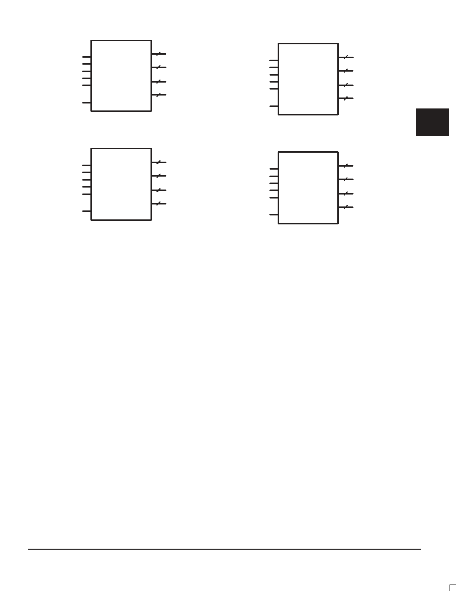
Figure 1. Dual Frequency Configuration
fsela
`1'
fselb
`1'
fselc
`1'
fseld
`0'
Input Ref
16.66MHz
66.66MHz
Qa
33.33MHz
Qb
33.33MHz
Qc
1
2
MPC950
Figure 2. Dual Frequency Configuration
`1'
`0'
`1'
Input Ref
33.33MHz
66.66MHz
Qa
66.66MHz
Qb
66.66MHz
Qc
1
2
FBsel
`0'
FBsel
`1'
fsela
fselb
fselc
fseld
66.66MHz
Qd
5
33.33MHz
Qd
5
MPC950
Figure 3. Dual Frequency Configuration
fsela
`1'
fselb
`1'
fselc
`1'
fseld
`1'
Input Ref
16.66MHz
66.66MHz
Qa
33.33MHz
Qb
33.33MHz
Qc
1
2
MPC950
Figure 4. Triple Frequency Configuration
`0'
`1'
Input Ref
20MHz
160MHz
Qa
80MHz
Qb
40MHz
Qc
1
2
FBsel
`0'
FBsel
`0'
fsela
fselb
fselc
fseld
33.33MHz
Qd
5
40MHz
Qd
5
Jitter Performance of the MPC950
With the clock rates of today’s digital systems continuing to
increase more emphasis is being placed on clock distribution
design and management. Among the issues being addressed
is system clock jitter and how that affects the overall system
timing budget. The MPC950 was designed to minimize clock
jitter by employing a differential bipolar PLL as well as incorpo-
rating numerous power and ground pins in the design. The
following few paragraphs will outline the jitter performance of
the MPC950, illustrate the measurement limitations and pro-
vide guidelines to minimize the jitter of the device.
The most commonly specified jitter parameter is cycle–to–
cycle jitter. Unfortunately with today’s high performance mea-
surement equipment there is no way to measure this parame-
ter for jitter performance in the class demonstrated by the
MPC950. As a result different methods are used which approx-
imate cycle–to–cycle jitter. The typical method of measuring
the jitter is to accumulate a large number of cycles, create a
histogram of the edge placements and record peak–to–peak
as well as standard deviations of the jitter. Care must be taken
that the measured edge is the edge immediately following the
trigger edge. If this is not the case the measurement inaccura-
cy will add significantly to the measured jitter. The oscilloscope
cannot collect adjacent pulses, rather it collects data from a
very large sample of pulses. It is safe to assume that collecting
pulse information in this mode will produce jitter values some-
what larger than if consecutive cycles were measured, there-
fore, this measurement will represent an upper bound of
cycle–to–cycle jitter. Most likely, this is a conservative estimate
of the cycle–to–cycle jitter.
There are two sources of jitter in a PLL based clock driver,
the commonly known random jitter of the PLL and the less
intuitive jitter caused by synchronous, different frequency out-
puts switching. For the case where all of the outputs are
switching at the same frequency the total jitter is exactly equal
to the PLL jitter. In a device, like the MPC950, where a number
of the outputs can be switching synchronously but at different
frequencies a “multi–modal” jitter distribution can be seen on
the highest frequency outputs. Because the output being moni-
tored is affected by the activity on the other outputs it is impor-
tant to consider what is happening on those other outputs.
From Figure 5, one can see for each rising edge on the higher
frequency signal the activity on the lower frequency signal is
not constant. The activity on the other outputs tends to alter the
internal thresholds of the device such that the placement of the
edge being monitored is displaced in time. Because the signals
are synchronous the relationship is periodic and the resulting
jitter is a compilation of the PLL jitter superimposed on the dis-
placed edges. When histograms are plotted the jitter looks like
a “multi–modal” distribution as pictured in Figure 5. Depending
on the size of the PLL jitter and the relative displacement of the
edges the “multi–modal” distribution will appear truly “multi–
modal” or simply like a “fat” Gaussian distribution. Again note
that in the case where all the outputs are switching at the same
frequency there is no edge displacement and the jitter is re-
duced to that of the PLL.
2
相关PDF资料 |
PDF描述 |
|---|---|
| MPC992FA | 375 MHz, PROC SPECIFIC CLOCK GENERATOR, PQFP32 |
| MPC992FA | 375 MHz, PROC SPECIFIC CLOCK GENERATOR, PQFP32 |
| MPD300-TR | SILICON, STABISTOR DIODE, DO-35 |
| MPN-7315-C11 | 150 V, SILICON, PIN DIODE |
| MPTE-15C | 1500 W, BIDIRECTIONAL, SILICON, TVS DIODE, DO-201AD |
相关代理商/技术参数 |
参数描述 |
|---|---|
| MPC951 | 制造商:MOTOROLA 制造商全称:Motorola, Inc 功能描述:LOW VOLTAGE PLL CLOCK DRIVER |
| MPC951FA | 制造商:Freescale Semiconductor 功能描述: 制造商:Motorola Inc 功能描述: |
| MPC951FAR2 | 制造商:Motorola Inc 功能描述: |
| MPC952 | 制造商:MOTOROLA 制造商全称:Motorola, Inc 功能描述:LOW VOLTAGE PLL CLOCK DRIVER |
| MPC953 | 制造商:MOTOROLA 制造商全称:Motorola, Inc 功能描述:LOW VOLTAGE PLL CLOCK DRIVER |
发布紧急采购,3分钟左右您将得到回复。