- 您现在的位置:买卖IC网 > PDF目录29137 > MPC973FA (INTEGRATED DEVICE TECHNOLOGY INC) 973 SERIES, PLL BASED CLOCK DRIVER, 12 TRUE OUTPUT(S), 0 INVERTED OUTPUT(S), PQFP52 PDF资料下载
参数资料
| 型号: | MPC973FA |
| 厂商: | INTEGRATED DEVICE TECHNOLOGY INC |
| 元件分类: | 时钟及定时 |
| 英文描述: | 973 SERIES, PLL BASED CLOCK DRIVER, 12 TRUE OUTPUT(S), 0 INVERTED OUTPUT(S), PQFP52 |
| 封装: | LQFP-52 |
| 文件页数: | 10/13页 |
| 文件大小: | 629K |
| 代理商: | MPC973FA |
MPC973
6
MOTOROLA
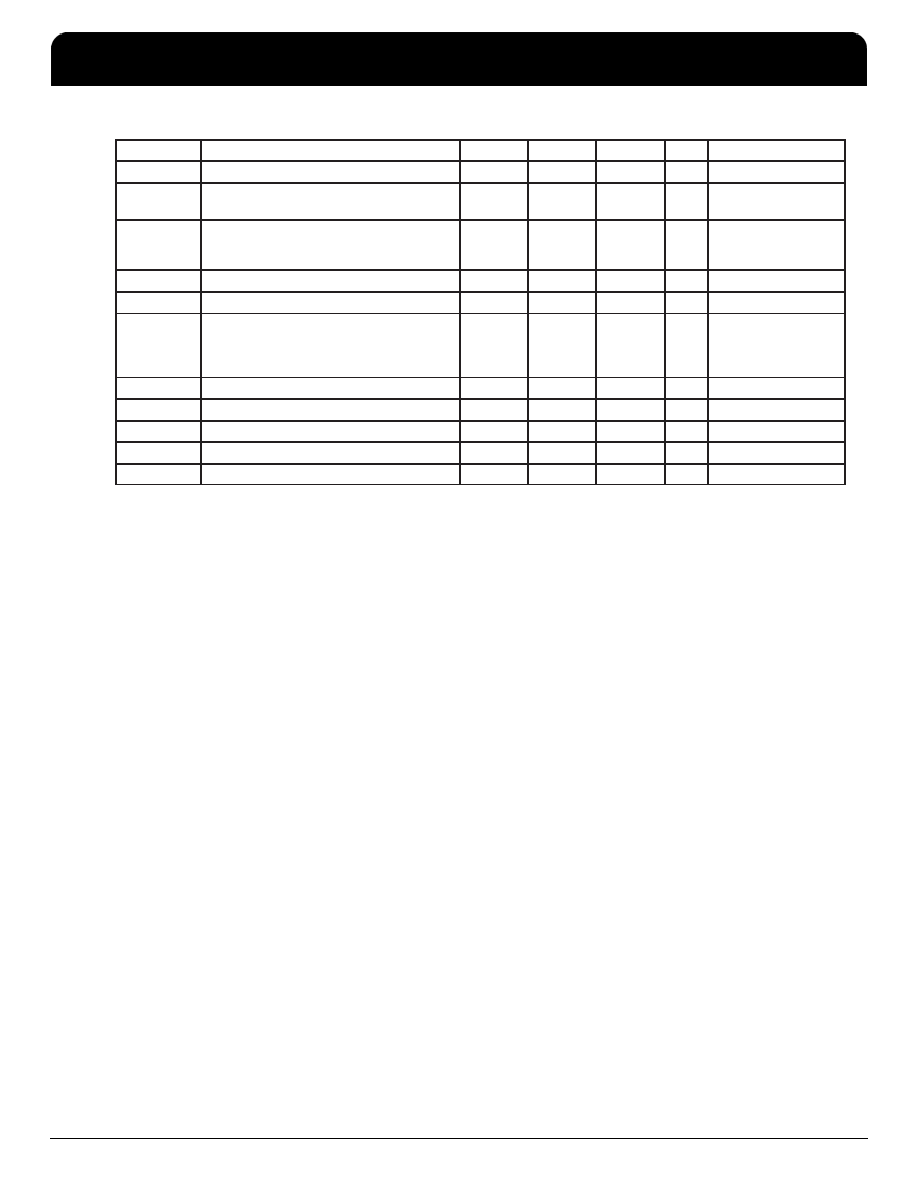
AC CHARACTERISTICS (TA = 0° to 70°C; VCC = 3.3V ±5%)
Symbol
Characteristic
Min
Typ
Max
Unit
Condition
tr, tf
Output Rise/Fall Time
0.15
1.2
ns
0.8 to 2.0V, Note 6.
tpw
Output Duty Cycle
tCYCLE/2
–750
tCYCLE/2
±500
tCYCLE/2
+750
ps
Note 6.
tpd
SYNC to Feedback
TCLK0
Propagation Delay
TCLK1
PCLK
–70
–130
–225
130
70
–25
330
270
175
ps
Notes 6., 7.; QFB =
÷8
tos
Output-to-Output Skew
550
ps
Note 6.
fVCO
VCO Lock Range
200
480
MHz
fmax
Maximum Output Frequency
Q (
÷2)
Q (
÷4)
Q (
÷6)
Q (
÷8)
125
120
80
60
MHz
Note 6.
tjitter
Cycle–to–Cycle Jitter (Peak–to–Peak)
±100
ps
Note 6.
tPLZ, tPHZ
Output Disable Time
2
8
ns
Note 6.
tPZL, tPZH
Output ENable TIme
2
10
ns
Note 6.
tlock
Maximum PLL Lock Time
10
ms
fMAX
Maximum Frz_Clk Frequency
20
MHz
6. 50
transmission line terminated into VCC/2.
7. tpd is specified for a 50MHz input reference. The window will shrink/grow proportionally from the minimum limit with shorter/longer input reference
periods. The tpd does not include jitter.
APPLICATIONS INFORMATION
Programming the MPC973
The MPC973 is the most flexible frequency programming
device in the Motorola timing solution portfolio. With three
independent banks of four outputs as well as an independent
PLL
feedback
output
the
total
number
of
possible
configurations is too numerous to tabulate. Table 1 tabulates
the various selection possibilities for the three banks of outputs.
The divide numbers presented in the table represent the divider
applied to the output of the VCO for that bank of outputs. To
determine the relationship between the three banks the three
divide ratios would be compared. For instance if a frequency
relationship of 5:3:2 was desired the following selection could
be made. The Qb outputs could be set to
÷10, the Qa outputs
to
÷6 and the Qc outputs to ÷4. With this output divide selection
the desired 5:3:2 relationship would be generated. For
situations where the VCO will run at relatively low frequencies
the PLL may not be stable for the desired divide ratios. For
these circumstances the VCO_Sel pin allows for an extra
÷2 to
be added into the clock path. When asserted this pin will
maintain the desired output relationships, but will provide an
enhanced lock range for the PLL. Once the output frequency
relationship is set and the VCO is in its stable range the
feedback output would be programmed to match the input
reference frequency.
The MPC973 offers only an external feedback to the PLL. A
separate feedback output is provided to optimize the flexibility
of the device. If in the example above the input reference
frequency was equal to the lowest output frequency the
feedback output would be set in the
÷10 mode. If the input
needed to be half the lowest frequency output the fselFB2 input
could be asserted to halve the feedback frequency. This action
multiplies the output frequencies by two relative to the input
reference frequency. With 7 unique feedback divide capabilities
there is a tremendous amount of flexibility. Again assume the
above 5:3:2 relationship is needed with the highest frequency
output equal to 100 MHz. If one was also constrained because
the only reference frequency available was 50MHz the setup in
figure 8 could be used. The MPC973 provides the 100, 66 and
40MHz outputs all synthesized from the 50 MHz source. With
its multitude of divide ratio capabilities the MPC973 can
generate almost any frequency from a standard, common
frequency already present in a design. Figures 9 and 10
illustrate a few more examples of possible MPC973
configurations.
The MPC973 has one more programming feature added to
its arsenal. The Inv_Clk input pin when asserted will invert the
Qc2 and Qc3 outputs. This inversion will not affect the
output–output skew of the device. This inversion allows for the
development of 180
° phase shifted clocks. This output could
also be used as a feedback output to the MPC973 or a second
PLL device to generate early or late clocks for a specific design.
Figure 11 illustrates the use of two MPC973’s to generate two
banks of clocks with one bank divided by 2 and delayed by 180
°
relative to the first.
F
re
e
sc
a
le
S
e
m
ic
o
n
d
u
c
to
r,
I
Freescale Semiconductor, Inc.
For More Information On This Product,
Go to: www.freescale.com
n
c
..
.
MPC973
Low Voltage PLL Clock Driver
NETCOM
IDT Low Voltage PLL Clock Driver
Freescale Timing Solutions Organization has been acquired by Integrated Device Technology, Inc
MPC973
6
相关PDF资料 |
PDF描述 |
|---|---|
| MPC974FAR2 | 974 SERIES, PLL BASED CLOCK DRIVER, 14 TRUE OUTPUT(S), 0 INVERTED OUTPUT(S), PQFP52 |
| MPC974FA | 974 SERIES, PLL BASED CLOCK DRIVER, 14 TRUE OUTPUT(S), 0 INVERTED OUTPUT(S), PQFP52 |
| MPC974FA | 974 SERIES, PLL BASED CLOCK DRIVER, 14 TRUE OUTPUT(S), 0 INVERTED OUTPUT(S), PQFP52 |
| MPC9773AE | 9773 SERIES, PLL BASED CLOCK DRIVER, 12 TRUE OUTPUT(S), 0 INVERTED OUTPUT(S), PQFP52 |
| MPC97H74AER2 | 97H SERIES, PLL BASED CLOCK DRIVER, 14 TRUE OUTPUT(S), 0 INVERTED OUTPUT(S), PQFP52 |
相关代理商/技术参数 |
参数描述 |
|---|---|
| MPC974 | 制造商:MOTOROLA 制造商全称:Motorola, Inc 功能描述:LOW VOLTAGE PLL CLOCK DRIVER |
| MPC974A44 F44A WAF | 制造商:Motorola Inc 功能描述: |
| MPC9772 | 制造商:MOTOROLA 制造商全称:Motorola, Inc 功能描述:3.3V 1:12 LVCMOS PLL Clock Generator |
| MPC9772AE | 功能描述:锁相环 - PLL 2.5 3.3V 250MHz Clock Generator RoHS:否 制造商:Silicon Labs 类型:PLL Clock Multiplier 电路数量:1 最大输入频率:710 MHz 最小输入频率:0.002 MHz 输出频率范围:0.002 MHz to 808 MHz 电源电压-最大:3.63 V 电源电压-最小:1.71 V 最大工作温度:+ 85 C 最小工作温度:- 40 C 封装 / 箱体:QFN-36 封装:Tray |
| MPC9772AER2 | 功能描述:时钟发生器及支持产品 FSL 1-12 LVCMOS PLL Clock Generator, xta RoHS:否 制造商:Silicon Labs 类型:Clock Generators 最大输入频率:14.318 MHz 最大输出频率:166 MHz 输出端数量:16 占空比 - 最大:55 % 工作电源电压:3.3 V 工作电源电流:1 mA 最大工作温度:+ 85 C 安装风格:SMD/SMT 封装 / 箱体:QFN-56 |
发布紧急采购,3分钟左右您将得到回复。