- 您现在的位置:买卖IC网 > PDF目录29137 > MPC9773AE (INTEGRATED DEVICE TECHNOLOGY INC) 9773 SERIES, PLL BASED CLOCK DRIVER, 12 TRUE OUTPUT(S), 0 INVERTED OUTPUT(S), PQFP52 PDF资料下载
参数资料
| 型号: | MPC9773AE |
| 厂商: | INTEGRATED DEVICE TECHNOLOGY INC |
| 元件分类: | 时钟及定时 |
| 英文描述: | 9773 SERIES, PLL BASED CLOCK DRIVER, 12 TRUE OUTPUT(S), 0 INVERTED OUTPUT(S), PQFP52 |
| 封装: | 10 X 10 MM, 1.40 MM HEIGHT, 0.65 MM PITCH, LEAD FREE, LQFP-52 |
| 文件页数: | 18/19页 |
| 文件大小: | 1007K |
| 代理商: | MPC9773AE |
Advanced Clock Drivers Device Data
8
Freescale Semiconductor
MPC9773
APPLICATIONS INFORMATION
MPC9773 Configurations
Configuring the MPC9773 amounts to properly configuring
the internal dividers to produce the desired output
frequencies. The output frequency can be represented by
this formula:
where fREF is the reference frequency of the selected input
clock source (CCLKO, CCLK1 or PCLK), M is the PLL
feedback divider and N is an output divider. The PLL
feedback divider is configured by the FSEL_FB[2:0] and the
output dividers are individually configured for each output
bank by the FSEL_A[1:0], FSEL_B[1:0] and FSEL_C[1:0]
inputs.
The reference frequency fREF and the selection of the
feedback-divider M is limited by the specified VCO frequency
range. fREF and M must be configured to match the VCO
frequency range of 200 to 480 MHz in order to achieve stable
PLL operation:
fVCO,MIN ≤ (fREF VCO_SEL M) ≤ fVCO,MAX
The PLL post-divider VCO_SEL is either a divide-by-one
or a divide-by-two and can be used to situate the VCO into
the specified frequency range. This divider is controlled by
the VCO_SEL pin. VCO_SEL effectively extends the usable
input frequency range while it has no effect on the output to
reference frequency ratio.
The output frequency for each bank can be derived from
the VCO frequency and output divider:
fQA[0:3] = fVCO ÷ (VCO_SEL NA)
fQB[0:3] = fVCO ÷ (VCO_SEL NB)
fQC[0:3] = fVCO ÷ (VCO_SEL NC)
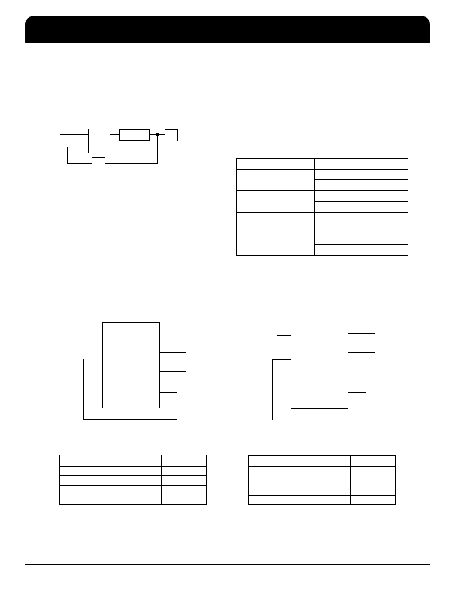
Table 11 shows the various PLL feedback and output
dividers, and Figure 3 and Figure 4 display example
configurations for the MPC9773.
Figure 3. Example Configuration
Figure 4. Example Configuration
÷VCO_SEL
÷M
÷N
fREF
fOUT
fOUT = fREF M ÷ N
PLL
Table 11. MPC9773 Divider
Divider
Function
VCO_SEL
Values
M
PLL Feedback
FSEL_FB[0:3]
÷1
4, 6, 8, 10, 12, 16
÷2
8, 12, 16, 20, 24, 32, 40
NA
Bank A Output
Divider FSEL_A[0:1]
÷1
4, 6, 8, 12
÷2
8, 12, 16, 24
NB
Bank B Output
Divider FSEL_B[0:1]
÷1
4, 6, 8, 10
÷2
8, 12, 16, 20
NC
Bank C Output
Divider FSEL_C[0:1]
÷1
2, 4, 6, 8
÷2
4, 8, 12, 16
MPC9773
fREF = 33.3 MHz
33.3 MHz
100 MHz
33.3 MHz (Feedback)
200 MHz
CCLK0
VCO_SEL
FSEL_A[1:0]
FSEL_B[1:0]
FSEL_C[1:0]
FSEL_FB[2:0]
QA[3:0]
QB[3:0]
QC[3:0]
QFB
CCLK1
CCLK_SEL
FB_IN
1
11
00
101
MPC9773 example configuration (feedback of
QFB = 33.3 MHz, fVCO = 400 MHz, VCO_SEL = ÷1,
M = 12, NA = 12, NB = 4, NC = 2).
Frequency Range
Min
Max
Input
16.6 MHz
40 MHz
QA outputs
16.6 MHz
40 MHz
QB outputs
50 MHz
120 MHz
QC outputs
100 MHz
240 MHz
MPC9773
fREF = 25 MHz
62.5 MHz
25 MHz (Feedback)
125 MHz
CCLK0
VCO_SEL
FSEL_A[1:0]
FSEL_B[1:0]
FSEL_C[1:0]
FSEL_FB[2:0]
QA[3:0]
QB[3:0]
QC[3:0]
QFB
CCLK1
CCLK_SEL
FB_IN
1
00
011
MPC9773 example configuration (feedback of
QFB = 25 MHz, fVCO = 250 MHz, VCO_SEL = ÷1,
M = 10, NA = 4, NB = 4, NC = 2).
Frequency Range
Min
Max
Input
20 MHz
48 MHz
QA outputs
50 MHz
120 MHz
QB outputs
50 MHz
120 MHz
QC outputs
100 MHz
240 MHz
MPC9773
3.3 V 1:12 LVCMOS PLL Clock Generator
NETCOM
IDT 3.3 V 1:12 LVCMOS PLL Clock Generator
Freescale Timing Solutions Organization has been acquired by Integrated Device Technology, Inc
MPC9773
8
相关PDF资料 |
PDF描述 |
|---|---|
| MPC97H74AER2 | 97H SERIES, PLL BASED CLOCK DRIVER, 14 TRUE OUTPUT(S), 0 INVERTED OUTPUT(S), PQFP52 |
| MPC97H74FAR2 | 97H SERIES, PLL BASED CLOCK DRIVER, 14 TRUE OUTPUT(S), 0 INVERTED OUTPUT(S), PQFP52 |
| MPC97H74FA | 97H SERIES, PLL BASED CLOCK DRIVER, 14 TRUE OUTPUT(S), 0 INVERTED OUTPUT(S), PQFP52 |
| MPC9893FAR2 | 9893 SERIES, PLL BASED CLOCK DRIVER, 12 TRUE OUTPUT(S), 0 INVERTED OUTPUT(S), PQFP48 |
| MPC991FAR2 | PLL BASED CLOCK DRIVER, 13 TRUE OUTPUT(S), 0 INVERTED OUTPUT(S), PQFP52 |
相关代理商/技术参数 |
参数描述 |
|---|---|
| MPC9773AER2 | 功能描述:时钟发生器及支持产品 FSL 1-12 LVCMOS/LVPE CL to LVCMOS PLL Clo RoHS:否 制造商:Silicon Labs 类型:Clock Generators 最大输入频率:14.318 MHz 最大输出频率:166 MHz 输出端数量:16 占空比 - 最大:55 % 工作电源电压:3.3 V 工作电源电流:1 mA 最大工作温度:+ 85 C 安装风格:SMD/SMT 封装 / 箱体:QFN-56 |
| MPC9773FA | 功能描述:锁相环 - PLL 3.3V 240MHz Clock Generator RoHS:否 制造商:Silicon Labs 类型:PLL Clock Multiplier 电路数量:1 最大输入频率:710 MHz 最小输入频率:0.002 MHz 输出频率范围:0.002 MHz to 808 MHz 电源电压-最大:3.63 V 电源电压-最小:1.71 V 最大工作温度:+ 85 C 最小工作温度:- 40 C 封装 / 箱体:QFN-36 封装:Tray |
| MPC9773FAR2 | 制造商:Integrated Device Technology Inc 功能描述:PLL Clock Driver Single 52-Pin LQFP T/R 制造商:Integrated Device Technology Inc 功能描述:MPC9773FAR2 - Tape and Reel |
| MPC9774 | 制造商:MOTOROLA 制造商全称:Motorola, Inc 功能描述:3.3V / 2,5V 1:14 LVCMOS PLL CLOCK GENERATOR |
| MPC9774AE | 功能描述:时钟发生器及支持产品 3.3V 125MHz Clock Generator RoHS:否 制造商:Silicon Labs 类型:Clock Generators 最大输入频率:14.318 MHz 最大输出频率:166 MHz 输出端数量:16 占空比 - 最大:55 % 工作电源电压:3.3 V 工作电源电流:1 mA 最大工作温度:+ 85 C 安装风格:SMD/SMT 封装 / 箱体:QFN-56 |
发布紧急采购,3分钟左右您将得到回复。