- 您现在的位置:买卖IC网 > PDF目录262872 > MSC1210Y4PAGR (TEXAS INSTRUMENTS INC) 8-BIT, FLASH, 33 MHz, MICROCONTROLLER, PQFP64 PDF资料下载
参数资料
| 型号: | MSC1210Y4PAGR |
| 厂商: | TEXAS INSTRUMENTS INC |
| 元件分类: | 微控制器/微处理器 |
| 英文描述: | 8-BIT, FLASH, 33 MHz, MICROCONTROLLER, PQFP64 |
| 封装: | GREEN, PLASTIC, TQFP-64 |
| 文件页数: | 24/94页 |
| 文件大小: | 913K |
| 代理商: | MSC1210Y4PAGR |
第1页第2页第3页第4页第5页第6页第7页第8页第9页第10页第11页第12页第13页第14页第15页第16页第17页第18页第19页第20页第21页第22页第23页当前第24页第25页第26页第27页第28页第29页第30页第31页第32页第33页第34页第35页第36页第37页第38页第39页第40页第41页第42页第43页第44页第45页第46页第47页第48页第49页第50页第51页第52页第53页第54页第55页第56页第57页第58页第59页第60页第61页第62页第63页第64页第65页第66页第67页第68页第69页第70页第71页第72页第73页第74页第75页第76页第77页第78页第79页第80页第81页第82页第83页第84页第85页第86页第87页第88页第89页第90页第91页第92页第93页第94页
MSC1210
SBAS203J MARCH 2002 REVISED JANUARY 2008
www.ti.com
30
The MSC1210 allows the user to partition the Flash
Memory between Program Memory and Data Memory. For
instance, the MSC1210Y5 contains 32kB of Flash
Memory on-chip. Through the HW configuration registers,
the user can define the partition between Program
Memory (PM) and Data Memory (DM), as shown in Table 3
and Table 4. The MSC1210 family offers four memory
configurations, as shown.
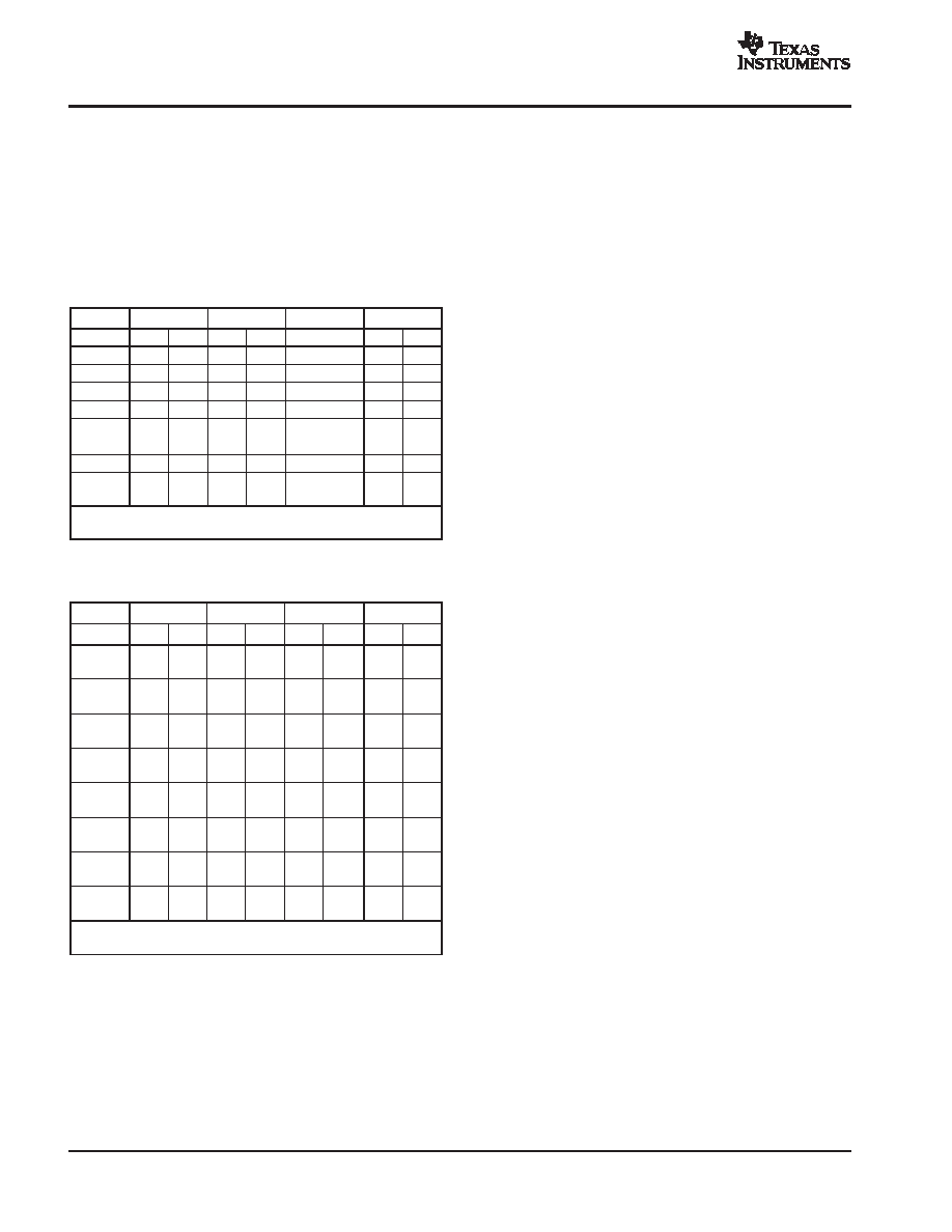
Table 3. MSC1210 Flash Partitioning
HCR0
MSC1210Y2
MSC1210Y3
MSC1210Y4
MSC1210Y5
DFSEL
PM
DM
PM
DM
PM
DM
PM
DM
000
0kB
4kB
0kB
8kB
0kB
16kB
0kB
32kB
001
0kB
4kB
0kB
8kB
0kB
16kB
0kB
32kB
010
0kB
4kB
0kB
8kB
0kB
16kB
011
0kB
4kB
0kB
8kB
24kB
8kB
100
0kB
4kB
12kB
4kB
28kB
4kB
101
2kB
6kB
2kB
14kB
2kB
30kB
2kB
110
3kB
1kB
7kB
1kB
15kB
1kB
31kB
1kB
111
(default)
4kB
0kB
8kB
0kB
16kB
0kB
32kB
0kB
NOTE: When a 0kB program memory configuration is selected, program
execution is external.
Table 4. MSC1210 Flash Memory Partitioning
HCR0
MSC1210Y2
MSC1210Y3
MSC1210Y4
MSC1210Y5
DFSEL
PM
DM
PM
DM
PM
DM
PM
DM
000
0000
0400-
13FF
0000
0400-
23FF
0000
0400-
43FF
0000
0400-
83FF
001
0000
0400-
13FF
0000
0400-
23FF
0000
0400-
43FF
0000
0400-
83FF
010
0000
0400-
13FF
0000
0400-
23FF
0000
0400-
43FF
0000-
3FFF
0400-
43FF
011
0000
0400-
13FF
0000
0400-
23FF
0000-
1FFF
0400-
23FF
0000-
5FFF
0400-
23FF
100
0000
0400-
13FF
0000-
0FFF
0400-
13FF
0000-
2FFF
0400-
13FF
0000-
6FFF
0400-
13FF
101
0000-
07FF
0400-
0BFF
0000-
17FF
0400-
0BFF
0000-
37FF
0400-
0BFF
0000-
77FF
0400-
0BFF
110
0000-
0BFF
0400-
07FF
0000-
1BFF
0400-
07FF
0000-
3BFF
0400-
07FF
0000-
7BFF
0400-
07FF
111
(default)
0000-
0FFF
0000
0000-
1FFF
0000
0000-
3FFF
0000
0000-
7FFF
0000
NOTE: Program memory accesses above the highest listed address will
access external program memory.
It is important to note that the Flash Memory is readable
and writable by the user through the MOVX instruction
when configured as either Program or Data Memory (via
the MXWS bit in the MWS, SFR 8Fh). This means that the
user may partition the device for maximum Flash Program
Memory size (no Flash Data Memory) and use Flash
Program Memory as Flash Data Memory. This may lead to
undesirable behavior if the PC points to an area of Flash
Program Memory that is being used for data storage.
Therefore, it is recommended to use Flash partitioning
when Flash Memory is used for data storage. Flash
partitioning prohibits execution of code from Data Flash
Memory. Additionally, the Program Memory erase/write
can be disabled through hardware configuration bits
(HCR0), while still providing access (read/write/erase) to
Data Flash Memory.
The effect of memory mapping on Program and Data
Memory is straightforward. The Program Memory is
decreased in size from the top of internal Program
Memory. Therefore, if the MSC1210Y5 is partitioned with
31kB of Flash Program Memory and 1kB of Flash Data
Memory, external Program Memory execution will begin at
7C00h (versus 8000h for 32kB). The Flash Data Memory
is added on top of the SRAM memory. Therefore, access
to Data Memory (through MOVX) will access SRAM for
addresses 0000h03FFh and access Flash Memory for
addresses 0400h07FFh.
Data Memory
The MSC1210 can address 64kB of Data Memory. The
MOVX instruction is used to access the Data SRAM
Memory. This includes 1,024 bytes of on-chip Data SRAM
Memory. The data bus values do not appear on Port 0
(during data bus timing) for internal memory access.
The MSC1210 also has on-chip Flash Data Memory which
is readable and writable (depending on Memory Write
Select register) during normal operation (full VDD range).
This memory is mapped into the external Data Memory
space directly above the SRAM.
The MOVX instruction is used to write the flash memory.
Flash memory must be erased before it can be written.
Flash memory is erased in 128 byte pages.
相关PDF资料 |
PDF描述 |
|---|---|
| M38503M4A-XXXFP | 8-BIT, MROM, 12.5 MHz, MICROCONTROLLER, PDSO42 |
| M38K27M4-XXXFP | 8-BIT, MROM, 8 MHz, MICROCONTROLLER, PQFP64 |
| M30101M2-XXXFP | 16-BIT, MROM, 16 MHz, MICROCONTROLLER, PDSO42 |
| MSP430F437IPZR | 16-BIT, FLASH, 8 MHz, RISC MICROCONTROLLER, PQFP100 |
| MC68HC05CC1B | 8-BIT, MROM, 4.2 MHz, MICROCONTROLLER, PDIP42 |
相关代理商/技术参数 |
参数描述 |
|---|---|
| MSC1210Y4PAGRG4 | 功能描述:模数转换器 - ADC Prec ADC w/ 8051 Mcntrl & Flash RoHS:否 制造商:Texas Instruments 通道数量:2 结构:Sigma-Delta 转换速率:125 SPs to 8 KSPs 分辨率:24 bit 输入类型:Differential 信噪比:107 dB 接口类型:SPI 工作电源电压:1.7 V to 3.6 V, 2.7 V to 5.25 V 最大工作温度:+ 85 C 安装风格:SMD/SMT 封装 / 箱体:VQFN-32 |
| MSC1210Y4PAGT | 功能描述:模数转换器 - ADC Prec ADC w/ 8051 Mcntrl & Flash RoHS:否 制造商:Texas Instruments 通道数量:2 结构:Sigma-Delta 转换速率:125 SPs to 8 KSPs 分辨率:24 bit 输入类型:Differential 信噪比:107 dB 接口类型:SPI 工作电源电压:1.7 V to 3.6 V, 2.7 V to 5.25 V 最大工作温度:+ 85 C 安装风格:SMD/SMT 封装 / 箱体:VQFN-32 |
| MSC1210Y4PAGTG4 | 功能描述:模数转换器 - ADC Prec ADC w/ 8051 Mcntrl & Flash RoHS:否 制造商:Texas Instruments 通道数量:2 结构:Sigma-Delta 转换速率:125 SPs to 8 KSPs 分辨率:24 bit 输入类型:Differential 信噪比:107 dB 接口类型:SPI 工作电源电压:1.7 V to 3.6 V, 2.7 V to 5.25 V 最大工作温度:+ 85 C 安装风格:SMD/SMT 封装 / 箱体:VQFN-32 |
| MSC1210Y5 | 制造商:TI 制造商全称:Texas Instruments 功能描述:Precision Analog-to-Digital Converter (ADC) with 8051 Microcontroller and Flash Memory |
| MSC1210Y5PAGR | 功能描述:模数转换器 - ADC Prec ADC w/ 8051 Mcntrl & Flash RoHS:否 制造商:Texas Instruments 通道数量:2 结构:Sigma-Delta 转换速率:125 SPs to 8 KSPs 分辨率:24 bit 输入类型:Differential 信噪比:107 dB 接口类型:SPI 工作电源电压:1.7 V to 3.6 V, 2.7 V to 5.25 V 最大工作温度:+ 85 C 安装风格:SMD/SMT 封装 / 箱体:VQFN-32 |
发布紧急采购,3分钟左右您将得到回复。