- 您现在的位置:买卖IC网 > PDF目录1955 > MSC7119VM1200 (Freescale Semiconductor)DSP 16BIT W/DDR CTRLR 400-MAPBGA PDF资料下载
参数资料
| 型号: | MSC7119VM1200 |
| 厂商: | Freescale Semiconductor |
| 文件页数: | 20/60页 |
| 文件大小: | 0K |
| 描述: | DSP 16BIT W/DDR CTRLR 400-MAPBGA |
| 标准包装: | 90 |
| 系列: | StarCore |
| 类型: | 定点 |
| 接口: | 主机接口,I²C,UART |
| 时钟速率: | 300MHz |
| 非易失内存: | ROM(8 kB) |
| 芯片上RAM: | 464kB |
| 电压 - 输入/输出: | 3.30V |
| 电压 - 核心: | 1.20V |
| 工作温度: | -40°C ~ 105°C |
| 安装类型: | 表面贴装 |
| 封装/外壳: | 400-LFBGA |
| 供应商设备封装: | 400-MAPBGA(17x17) |
| 包装: | 托盘 |
第1页第2页第3页第4页第5页第6页第7页第8页第9页第10页第11页第12页第13页第14页第15页第16页第17页第18页第19页当前第20页第21页第22页第23页第24页第25页第26页第27页第28页第29页第30页第31页第32页第33页第34页第35页第36页第37页第38页第39页第40页第41页第42页第43页第44页第45页第46页第47页第48页第49页第50页第51页第52页第53页第54页第55页第56页第57页第58页第59页第60页
Electrical Characteristics
MSC7119 Data Sheet, Rev. 8
Freescale Semiconductor
27
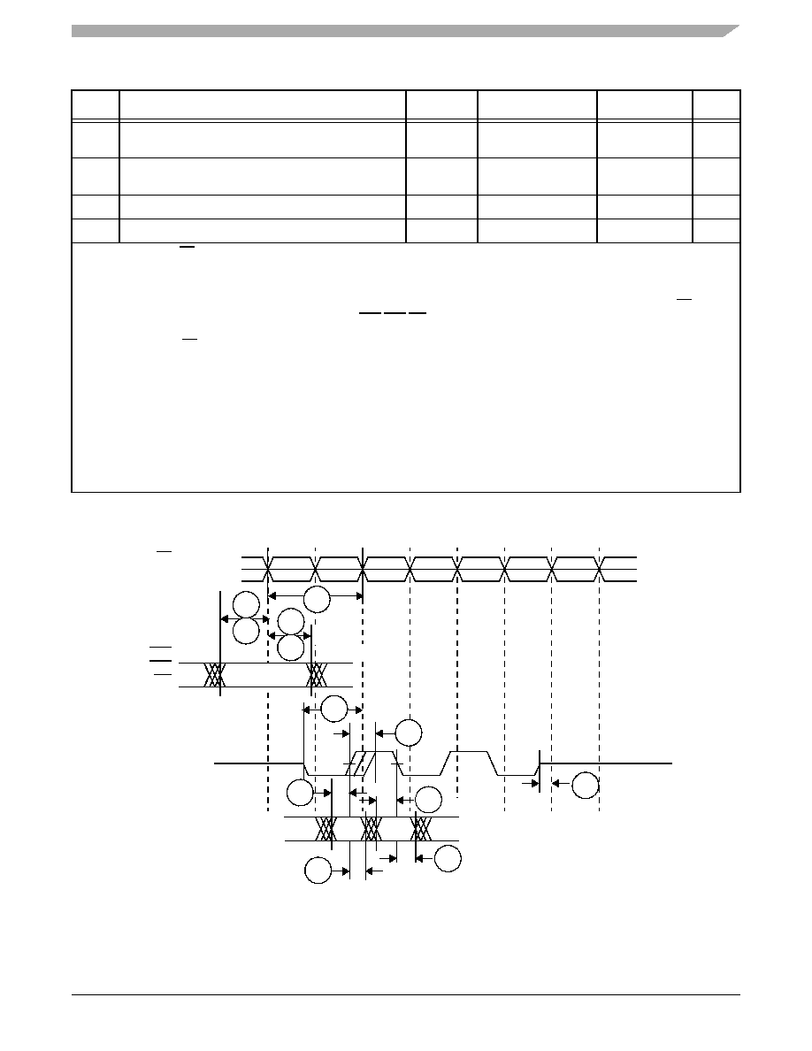
Figure 6 shows the DDR DRAM output timing diagram.
209
Dn/DQMn output setup with respect to DQSn3
tDDKHDS,
tDDKLDS
0.25
× tCK – 750
—
ps
210
Dn/DQMn output hold with respect to DQSn3
tDDKHDX,
tDDKLDX
0.25
× tCK – 750
—
ps
211
DQSn preamble start4
tDDKHMP
–0.25
× tCK
—ps
212
DQSn epilogue end5
tDDKHME
–600
600
ps
Notes:
1.
All CK/CK referenced measurements are made from the crossing of the two signals ±0.1 V.
2.
tDDKHMH can be modified through the TCFG2[WRDD] DQSS override bits. The DRAM requires that the first write data strobe
arrives 75–125% of a DRAM cycle after the write command is issued. Any skew between DQSn and CK must be considered
when trying to achieve this 75%–125% goal. The TCFG2[WRDD] bits can be used to shift DQSn by 1/4 DRAM cycle
increments. The skew in this case refers to an internal skew existing at the signal connections. By default, the CK/CK crossing
occurs in the middle of the control signal (An/RAS/CAS/WE/CKE) tenure. Setting TCFG2[ACSM] bit shifts the control signal
assertion 1/2 DRAM cycle earlier than the default timing. This means that the signal is asserted no earlier than 600 ps before
the CK/CK crossing and no later than 600 ps after the crossing time; the device uses 1200 ps of the skew budget (the interval
from –600 to +600 ps). Timing is verified by referencing the falling edge of CK. See Chapter 10 of the MSC711x Reference
Manual for details.
3.
Determined by maximum possible skew between a data strobe (DQS) and any corresponding bit of data. The data strobe
should be centered inside of the data eye.
4.
Please note that this spec is in reference to the DQSn first rising edge. It could also be referenced from CK(r), but due to
programmable delay of the write strobes (TCFG2[WRDD]), there pre-amble may be extended for a full DRAM cycle. For this
reason, we reference from DQSn.
5.
All outputs are referenced to the rising edge of CK. Note that this is essentially the CK/DQSn skew in spec 208. In addition
there is no real “maximum” time for the epilogue end. JEDEC does not require this is as a device limitation, but simply for the
chip to guarantee fast enough write-to-read turn-around times. This is already guaranteed by the memory controller operation.
Figure 6. DDR DRAM Output Timing Diagram
Table 18. DDR DRAM Output AC Timing (continued)
No.
Parameter
Symbol
Min
Max
Unit
An
Dn
DQSn
CK
D1
D0
Write A0
NOOP
RAS
CAS
WE
CKE
200
208
209
212
210
211
206
204
207
205
DQMn
相关PDF资料 |
PDF描述 |
|---|---|
| MSC8101M1500F | DSP 16BIT 300MHZ CPM 332-FCPBGA |
| MSC8101VT1500F | IC DSP 16BIT 250MHZ 332-FCPBGA |
| MSC8103M1200F | DSP 16BIT 300MHZ CPM 332-FCPBGA |
| MSC8103VT1200F | IC DSP 16BIT 300MHZ 332-FCPBGA |
| MSC8112TVT2400V | DSP DUAL CORE 431-FCPBGA |
相关代理商/技术参数 |
参数描述 |
|---|---|
| MSC711XADS | 功能描述:开发板和工具包 - 其他处理器 DEV SYS FOR FSL 711X DEV RoHS:否 制造商:Freescale Semiconductor 产品:Development Systems 工具用于评估:P3041 核心:e500mc 接口类型:I2C, SPI, USB 工作电源电压: |
| MSC711XEVM | 功能描述:开发板和工具包 - 其他处理器 EVAL KIT W/FULL LIC CW RoHS:否 制造商:Freescale Semiconductor 产品:Development Systems 工具用于评估:P3041 核心:e500mc 接口类型:I2C, SPI, USB 工作电源电压: |
| MSC711XEVMT | 功能描述:KIT EVAL W/FULL LIC CW RoHS:是 类别:编程器,开发系统 >> 过时/停产零件编号 系列:* 标准包装:1 系列:- 传感器类型:CMOS 成像,彩色(RGB) 传感范围:WVGA 接口:I²C 灵敏度:60 fps 电源电压:5.7 V ~ 6.3 V 嵌入式:否 已供物品:成像器板 已用 IC / 零件:KAC-00401 相关产品:4H2099-ND - SENSOR IMAGE WVGA COLOR 48-PQFP4H2094-ND - SENSOR IMAGE WVGA MONO 48-PQFP |
| MSC7121VRF | 制造商:Freescale Semiconductor 功能描述:GPON UMC 140 MHZ - Trays |
| MSC7128 | 制造商:OKI 制造商全称:OKI electronic componets 功能描述:5 x 7-Dot Character x 16-Digit Display Controller/Driver |
发布紧急采购,3分钟左右您将得到回复。