- 您现在的位置:买卖IC网 > PDF目录45388 > MSC8256SVT800B (FREESCALE SEMICONDUCTOR INC) 0-BIT, OTHER DSP, PBGA783 PDF资料下载
参数资料
| 型号: | MSC8256SVT800B |
| 厂商: | FREESCALE SEMICONDUCTOR INC |
| 元件分类: | 数字信号处理 |
| 英文描述: | 0-BIT, OTHER DSP, PBGA783 |
| 封装: | 29 X 29 MM, LEAD FREE, PLASTIC, FCBGA-783 |
| 文件页数: | 18/68页 |
| 文件大小: | 910K |
| 代理商: | MSC8256SVT800B |
第1页第2页第3页第4页第5页第6页第7页第8页第9页第10页第11页第12页第13页第14页第15页第16页第17页当前第18页第19页第20页第21页第22页第23页第24页第25页第26页第27页第28页第29页第30页第31页第32页第33页第34页第35页第36页第37页第38页第39页第40页第41页第42页第43页第44页第45页第46页第47页第48页第49页第50页第51页第52页第53页第54页第55页第56页第57页第58页第59页第60页第61页第62页第63页第64页第65页第66页第67页第68页
Electrical Characteristics
MSC8256 Six-Core Digital Signal Processor Data Sheet, Rev. 3
Freescale Semiconductor
25
Table 4 describes thermal characteristics of the MSC8256 for the FC-PBGA packages.
2.4
CLKIN Requirements
Table 5 summarizes the required characteristics for the CLKIN signal.
This section describes the DC electrical characteristics for the MSC8256.
2.5.1
DDR SDRAM DC Electrical Characteristics
This section describes the DC electrical specifications for the DDR SDRAM interface of the MSC8256.
Note:
DDR2 SDRAM uses VDDDDR(typ) = 1.8 V and DDR3 SDRAM uses VDDDDR(typ) = 1.5 V.
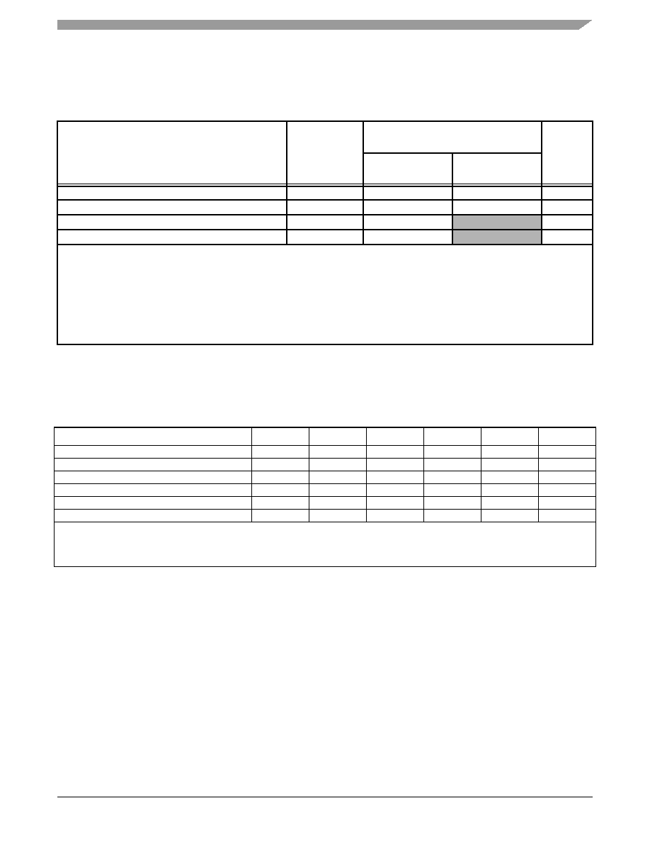
Table 4. Thermal Characteristics for the MSC8256
Characteristic
Symbol
FC-PBGA
29
× 29 mm2
Unit
Natural
Convection
200 ft/min
(1 m/s) airflow
Junction-to-ambient1, 2
RθJA
18
12
°C/W
Junction-to-ambient, four-layer board1, 2
RθJA
13
9
°C/W
Junction-to-board (bottom)3
RθJB
5
°C/W
Junction-to-case4
RθJC
0.6
°C/W
Notes:
1.
Junction temperature is a function of die size, on-chip power dissipation, package thermal resistance, mounting site (board)
temperature, ambient temperature, air flow, power dissipation of other components on the board, and board thermal
resistance.
2.
Junction-to-ambient thermal resistance determined per JEDEC JESD51-3 and JESDC51-6. Thermal test board meets JEDEC
specification for the specified package.
3.
Junction-to-board thermal resistance determined per JEDEC JESD 51-8. Thermal test board meets JEDEC specification for
the specified package.
4.
Junction-to-case at the top of the package determined using MIL- STD-883 Method 1012.1. The cold plate temperature is used
for the case temperature. Reported value includes the thermal resistance of the interface layer
Table 5. CLKIN Requirements
Parameter/Condition1
Symbol
Min
Typ
Max
Unit
Notes
CLKIN duty cycle
—
40
—
60
%
2
CLKIN slew rate
—
1
—
4
V/ns
3
CLKIN peak period jitter
—
±150
ps
—
CLKIN jitter phase noise at –56 dBc
—
500
KHz
4
AC input swing limits
ΔVAC
1.5
—
V
—
Input capacitance
CIN
——
15
pf
—
Notes:
1.
For clock frequencies, see the Clock chapter in the MSC8256 Reference Manual.
2.
Measured at the rising edge and/or the falling edge at VDDIO/2.
3.
Slew rate as measured from ±20% to 80% of voltage swing at clock input.
4.
Phase noise is calculated as FFT of TIE jitter.
相关PDF资料 |
PDF描述 |
|---|---|
| MSC8256TVT800B | 0-BIT, OTHER DSP, PBGA783 |
| MSC8256SVT1000B | 0-BIT, OTHER DSP, PBGA783 |
| MSM5547RS | 0 TIMER(S), REAL TIME CLOCK, PDIP42 |
| MSM58321RS | 0 TIMER(S), REAL TIME CLOCK, PDIP16 |
| MSM6052GS | 4-BIT, MROM, MICROCONTROLLER, PQFP44 |
相关代理商/技术参数 |
参数描述 |
|---|---|
| MSC8256TAG1000B | 制造商:Freescale Semiconductor 功能描述:STARCORE DSP, 6X 1GHZ SC3850 CORES, DDR2/3, SRIO, PCIE, QE, - Trays 制造商:Freescale Semiconductor 功能描述:IC DSP 6X 1GHZ SC3850 783FCBGA |
| MSC8256TVT1000B | 功能描述:数字信号处理器和控制器 - DSP, DSC DSPStarcore 6-core RoHS:否 制造商:Microchip Technology 核心:dsPIC 数据总线宽度:16 bit 程序存储器大小:16 KB 数据 RAM 大小:2 KB 最大时钟频率:40 MHz 可编程输入/输出端数量:35 定时器数量:3 设备每秒兆指令数:50 MIPs 工作电源电压:3.3 V 最大工作温度:+ 85 C 封装 / 箱体:TQFP-44 安装风格:SMD/SMT |
| MSC8256TVT800B | 功能描述:数字信号处理器和控制器 - DSP, DSC DSPStarcore 6-core RoHS:否 制造商:Microchip Technology 核心:dsPIC 数据总线宽度:16 bit 程序存储器大小:16 KB 数据 RAM 大小:2 KB 最大时钟频率:40 MHz 可编程输入/输出端数量:35 定时器数量:3 设备每秒兆指令数:50 MIPs 工作电源电压:3.3 V 最大工作温度:+ 85 C 封装 / 箱体:TQFP-44 安装风格:SMD/SMT |
| MSC83301 | 制造商:STMICROELECTRONICS 制造商全称:STMicroelectronics 功能描述:RF & MICROWAVE TRANSISTORS GENERAL PURPOSE AMPLIFIER APPLICATIONS |
| MSC83303 | 制造商:STMICROELECTRONICS 制造商全称:STMicroelectronics 功能描述:RF & MICROWAVE TRANSISTORS GENERAL PURPOSE AMPLIFIER APPLICATIONS |
发布紧急采购,3分钟左右您将得到回复。