- 您现在的位置:买卖IC网 > PDF目录45388 > MSC8256SVT800B (FREESCALE SEMICONDUCTOR INC) 0-BIT, OTHER DSP, PBGA783 PDF资料下载
参数资料
| 型号: | MSC8256SVT800B |
| 厂商: | FREESCALE SEMICONDUCTOR INC |
| 元件分类: | 数字信号处理 |
| 英文描述: | 0-BIT, OTHER DSP, PBGA783 |
| 封装: | 29 X 29 MM, LEAD FREE, PLASTIC, FCBGA-783 |
| 文件页数: | 25/68页 |
| 文件大小: | 910K |
| 代理商: | MSC8256SVT800B |
第1页第2页第3页第4页第5页第6页第7页第8页第9页第10页第11页第12页第13页第14页第15页第16页第17页第18页第19页第20页第21页第22页第23页第24页当前第25页第26页第27页第28页第29页第30页第31页第32页第33页第34页第35页第36页第37页第38页第39页第40页第41页第42页第43页第44页第45页第46页第47页第48页第49页第50页第51页第52页第53页第54页第55页第56页第57页第58页第59页第60页第61页第62页第63页第64页第65页第66页第67页第68页
Electrical Characteristics
MSC8256 Six-Core Digital Signal Processor Data Sheet, Rev. 3
Freescale Semiconductor
31
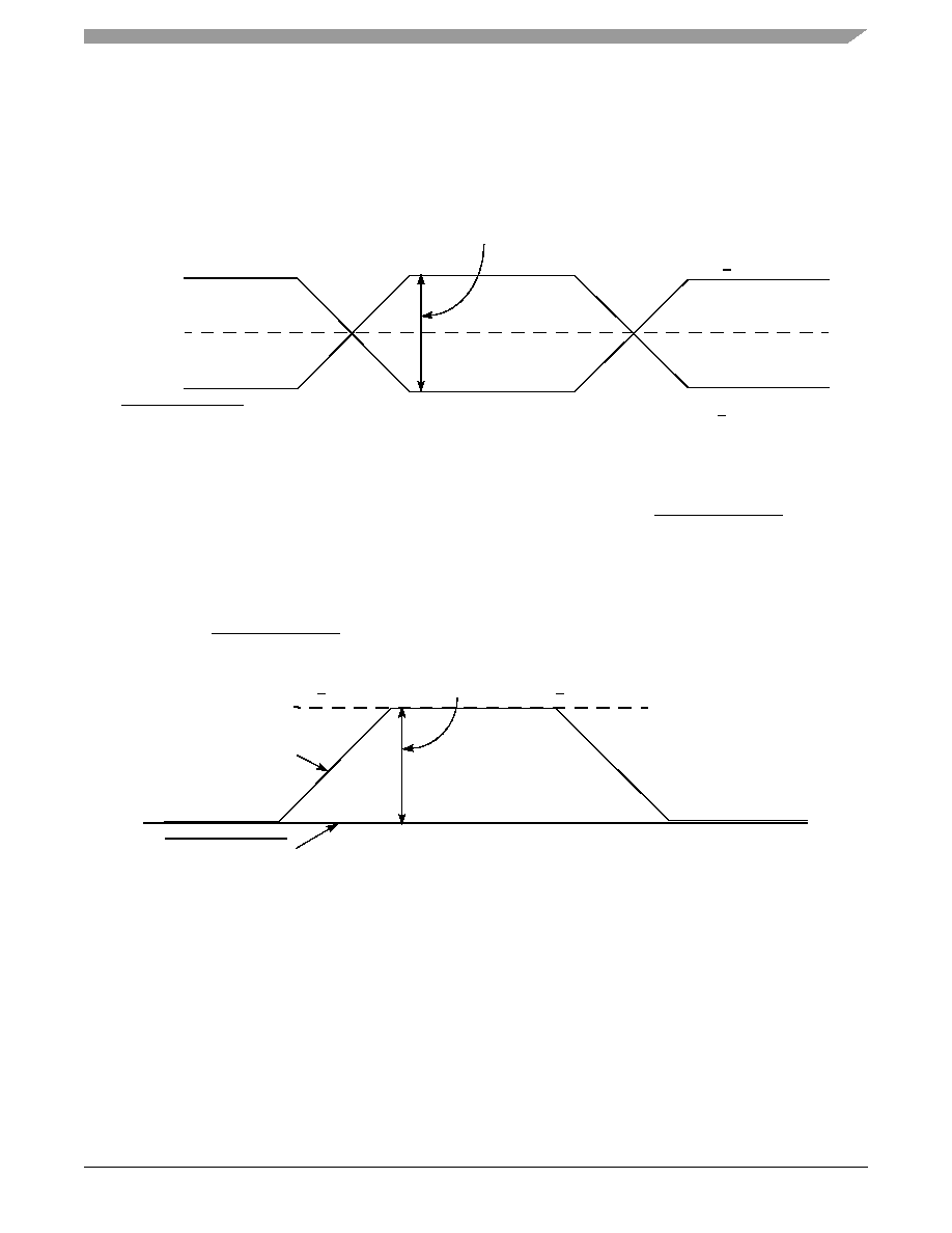
— For an external AC-coupled connection, there is no common mode voltage requirement for the clock driver.
Because the external AC-coupling capacitor blocks the DC-level, the clock driver and the SerDes reference clock
receiver operate in different command mode voltages. The SerDes reference clock receiver in this connection
scheme has its common mode voltage set to GNDSXC. Each signal wire of the differential inputs is allowed to
swing below and above the command mode voltage GNDSXC. Figure 8 shows the SerDes reference clock input
requirement for AC-coupled connection scheme.
Single-Ended Mode
— The reference clock can also be single-ended. The SR[1–2]_REF_CLK input amplitude (single-ended swing)
must be between 400 mV and 800 mV peak-peak (from VMIN to VMAX) with SR[1–2]_REF_CLK either left
unconnected or tied to ground.
— The SR[1–2]_REF_CLK input average voltage must be between 200 and 400 mV. Figure 9 shows the SerDes
reference clock input requirement for single-ended signaling mode.
— To meet the input amplitude requirement, the reference clock inputs may need to be DC- or AC-coupled
externally. For the best noise performance, the reference of the clock could be DC- or AC-coupled into the unused
phase (SR[1–2]_REF_CLK) through the same source impedance as the clock input (SR[1–2]_REF_CLK) in use.
2.5.3.2
DC-Level Requirements for PCI Express Configurations
The DC-level requirements for PCI Express implementations have separate requirements for the Tx and Rx lines. The
MSC8256 supports a 2.5 Gbps PCI Express interface defined by the PCI Express Base Specification, Revision 1.0a. The
transmitter specifications are defined in Table 11 and the receiver specifications are defined in Table 12.
Figure 8. Differential Reference Clock Input DC Requirements (External AC-Coupled)
Figure 9. Single-Ended Reference Clock Input DC Requirements
SR[1–2]_REF_CLK
Vcm
200 mV < Input Amplitude or Differential Peak < 800 mV
Vmax < Vcm + 400 mV
Vmin > Vcm – 400 mV
SR[1–2]_REF_CLK
400 mV < SR[1–2]_REF_CLK Input Amplitude < 800 mV
0V
相关PDF资料 |
PDF描述 |
|---|---|
| MSC8256TVT800B | 0-BIT, OTHER DSP, PBGA783 |
| MSC8256SVT1000B | 0-BIT, OTHER DSP, PBGA783 |
| MSM5547RS | 0 TIMER(S), REAL TIME CLOCK, PDIP42 |
| MSM58321RS | 0 TIMER(S), REAL TIME CLOCK, PDIP16 |
| MSM6052GS | 4-BIT, MROM, MICROCONTROLLER, PQFP44 |
相关代理商/技术参数 |
参数描述 |
|---|---|
| MSC8256TAG1000B | 制造商:Freescale Semiconductor 功能描述:STARCORE DSP, 6X 1GHZ SC3850 CORES, DDR2/3, SRIO, PCIE, QE, - Trays 制造商:Freescale Semiconductor 功能描述:IC DSP 6X 1GHZ SC3850 783FCBGA |
| MSC8256TVT1000B | 功能描述:数字信号处理器和控制器 - DSP, DSC DSPStarcore 6-core RoHS:否 制造商:Microchip Technology 核心:dsPIC 数据总线宽度:16 bit 程序存储器大小:16 KB 数据 RAM 大小:2 KB 最大时钟频率:40 MHz 可编程输入/输出端数量:35 定时器数量:3 设备每秒兆指令数:50 MIPs 工作电源电压:3.3 V 最大工作温度:+ 85 C 封装 / 箱体:TQFP-44 安装风格:SMD/SMT |
| MSC8256TVT800B | 功能描述:数字信号处理器和控制器 - DSP, DSC DSPStarcore 6-core RoHS:否 制造商:Microchip Technology 核心:dsPIC 数据总线宽度:16 bit 程序存储器大小:16 KB 数据 RAM 大小:2 KB 最大时钟频率:40 MHz 可编程输入/输出端数量:35 定时器数量:3 设备每秒兆指令数:50 MIPs 工作电源电压:3.3 V 最大工作温度:+ 85 C 封装 / 箱体:TQFP-44 安装风格:SMD/SMT |
| MSC83301 | 制造商:STMICROELECTRONICS 制造商全称:STMicroelectronics 功能描述:RF & MICROWAVE TRANSISTORS GENERAL PURPOSE AMPLIFIER APPLICATIONS |
| MSC83303 | 制造商:STMICROELECTRONICS 制造商全称:STMicroelectronics 功能描述:RF & MICROWAVE TRANSISTORS GENERAL PURPOSE AMPLIFIER APPLICATIONS |
发布紧急采购,3分钟左右您将得到回复。