- 您现在的位置:买卖IC网 > PDF目录45388 > MSC8256SVT800B (FREESCALE SEMICONDUCTOR INC) 0-BIT, OTHER DSP, PBGA783 PDF资料下载
参数资料
| 型号: | MSC8256SVT800B |
| 厂商: | FREESCALE SEMICONDUCTOR INC |
| 元件分类: | 数字信号处理 |
| 英文描述: | 0-BIT, OTHER DSP, PBGA783 |
| 封装: | 29 X 29 MM, LEAD FREE, PLASTIC, FCBGA-783 |
| 文件页数: | 32/68页 |
| 文件大小: | 910K |
| 代理商: | MSC8256SVT800B |
第1页第2页第3页第4页第5页第6页第7页第8页第9页第10页第11页第12页第13页第14页第15页第16页第17页第18页第19页第20页第21页第22页第23页第24页第25页第26页第27页第28页第29页第30页第31页当前第32页第33页第34页第35页第36页第37页第38页第39页第40页第41页第42页第43页第44页第45页第46页第47页第48页第49页第50页第51页第52页第53页第54页第55页第56页第57页第58页第59页第60页第61页第62页第63页第64页第65页第66页第67页第68页
MSC8256 Six-Core Digital Signal Processor Data Sheet, Rev. 3
Electrical Characteristics
Freescale Semiconductor
38
Note:
For the ADDR/CMD setup and hold specifications in Table 21, it is assumed that the clock control register is set to
adjust the memory clocks by applied cycle.
Notes:
1.
The symbols used for timing specifications follow the pattern of t(first two letters of functional block)(signal)(state) (reference)(state) for
inputs and t(first two letters of functional block)(reference)(state)(signal)(state) for outputs. Output hold time can be read as DDR timing
(DD) from the rising or falling edge of the reference clock (KH or KL) until the output went invalid (AX or DX). For example,
tDDKHAS symbolizes DDR timing (DD) for the time tMCK memory clock reference (K) goes from the high (H) state until outputs
(A) are setup (S) or output valid time. Also, tDDKLDX symbolizes DDR timing (DD) for the time tMCK memory clock reference (K)
goes low (L) until data outputs (D) are invalid (X) or data output hold time.
2.
All MCK/MCK referenced measurements are made from the crossing of the two signals.
3.
ADDR/CMD includes all DDR SDRAM output signals except MCK/MCK, MCS, and MDQ/MECC/MDM/MDQS.
4.
Note that tDDKHMH follows the symbol conventions described in note 1. For example, tDDKHMH describes the DDR timing (DD)
from the rising edge of the MCK(n) clock (KH) until the MDQS signal is valid (MH). tDDKHMH can be modified through control of
the DQSS override bits in the TIMING_CFG_2 register. This will typically be set to the same delay as the clock adjust in the
CLK_CNTL register. The timing parameters listed in the table assume that these two parameters have been set to the same
adjustment value. See the MSC8256 Reference Manual for a description and understanding of the timing modifications
enabled by use of these bits.
5.
Determined by maximum possible skew between a data strobe (MDQS) and any corresponding bit of data (MDQ), ECC
(MECC), or data mask (MDM). The data strobe should be centered inside of the data eye at the pins of the MSC8256.
6.
At recommended operating conditions with VDDDDR (1.5 V or 1,8 V) ± 5%.
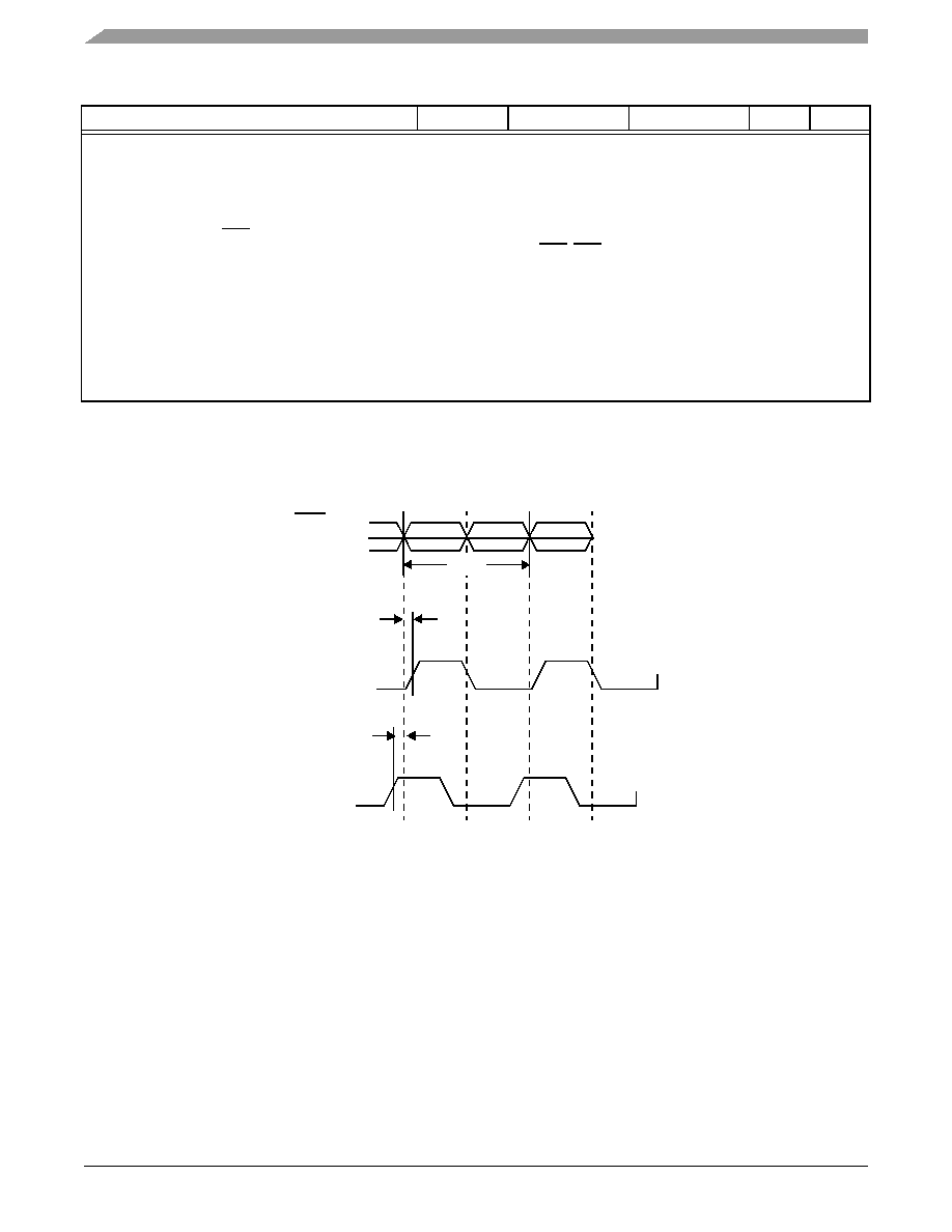
Figure 12. MCK to MDQS Timing
Table 21. DDR SDRAM Output AC Timing Specifications (continued)
Parameter
Symbol 1
Min
Max
Unit
Notes
MDQS
MCK[n]
tMCK
tDDKHMHmax) = 0.6 ns or 0.375 ns
tDDKHMH(min) = –0.6 ns or –0.375 ns
MDQS
相关PDF资料 |
PDF描述 |
|---|---|
| MSC8256TVT800B | 0-BIT, OTHER DSP, PBGA783 |
| MSC8256SVT1000B | 0-BIT, OTHER DSP, PBGA783 |
| MSM5547RS | 0 TIMER(S), REAL TIME CLOCK, PDIP42 |
| MSM58321RS | 0 TIMER(S), REAL TIME CLOCK, PDIP16 |
| MSM6052GS | 4-BIT, MROM, MICROCONTROLLER, PQFP44 |
相关代理商/技术参数 |
参数描述 |
|---|---|
| MSC8256TAG1000B | 制造商:Freescale Semiconductor 功能描述:STARCORE DSP, 6X 1GHZ SC3850 CORES, DDR2/3, SRIO, PCIE, QE, - Trays 制造商:Freescale Semiconductor 功能描述:IC DSP 6X 1GHZ SC3850 783FCBGA |
| MSC8256TVT1000B | 功能描述:数字信号处理器和控制器 - DSP, DSC DSPStarcore 6-core RoHS:否 制造商:Microchip Technology 核心:dsPIC 数据总线宽度:16 bit 程序存储器大小:16 KB 数据 RAM 大小:2 KB 最大时钟频率:40 MHz 可编程输入/输出端数量:35 定时器数量:3 设备每秒兆指令数:50 MIPs 工作电源电压:3.3 V 最大工作温度:+ 85 C 封装 / 箱体:TQFP-44 安装风格:SMD/SMT |
| MSC8256TVT800B | 功能描述:数字信号处理器和控制器 - DSP, DSC DSPStarcore 6-core RoHS:否 制造商:Microchip Technology 核心:dsPIC 数据总线宽度:16 bit 程序存储器大小:16 KB 数据 RAM 大小:2 KB 最大时钟频率:40 MHz 可编程输入/输出端数量:35 定时器数量:3 设备每秒兆指令数:50 MIPs 工作电源电压:3.3 V 最大工作温度:+ 85 C 封装 / 箱体:TQFP-44 安装风格:SMD/SMT |
| MSC83301 | 制造商:STMICROELECTRONICS 制造商全称:STMicroelectronics 功能描述:RF & MICROWAVE TRANSISTORS GENERAL PURPOSE AMPLIFIER APPLICATIONS |
| MSC83303 | 制造商:STMICROELECTRONICS 制造商全称:STMicroelectronics 功能描述:RF & MICROWAVE TRANSISTORS GENERAL PURPOSE AMPLIFIER APPLICATIONS |
发布紧急采购,3分钟左右您将得到回复。