- 您现在的位置:买卖IC网 > PDF目录224505 > MT29C2G24MAKLACG-75IT SPECIALTY MEMORY CIRCUIT, PBGA152 PDF资料下载
参数资料
| 型号: | MT29C2G24MAKLACG-75IT |
| 元件分类: | 存储器 |
| 英文描述: | SPECIALTY MEMORY CIRCUIT, PBGA152 |
| 封装: | GREEN, VFBGA-152 |
| 文件页数: | 14/15页 |
| 文件大小: | 421K |
| 代理商: | MT29C2G24MAKLACG-75IT |
PDF: 09005aef8326e5ac / Source: 09005aef8326e59a
Micron Technology, Inc., reserves the right to change products or specifications without notice.
152ball_ nand_lpdram_j4xx_omap.fm - Rev. E 4/09 EN
8
2008 Micron Technology, Inc. All rights reserved.
152-Ball NAND Flash and Mobile LPDRAM PoP (TI OMAP) MCP
Ball Assignments and Descriptions
Preliminary
Notes: 1. Balls marked RFU may or may not be connected internally. These balls should not be used.
Contact the factory for details.
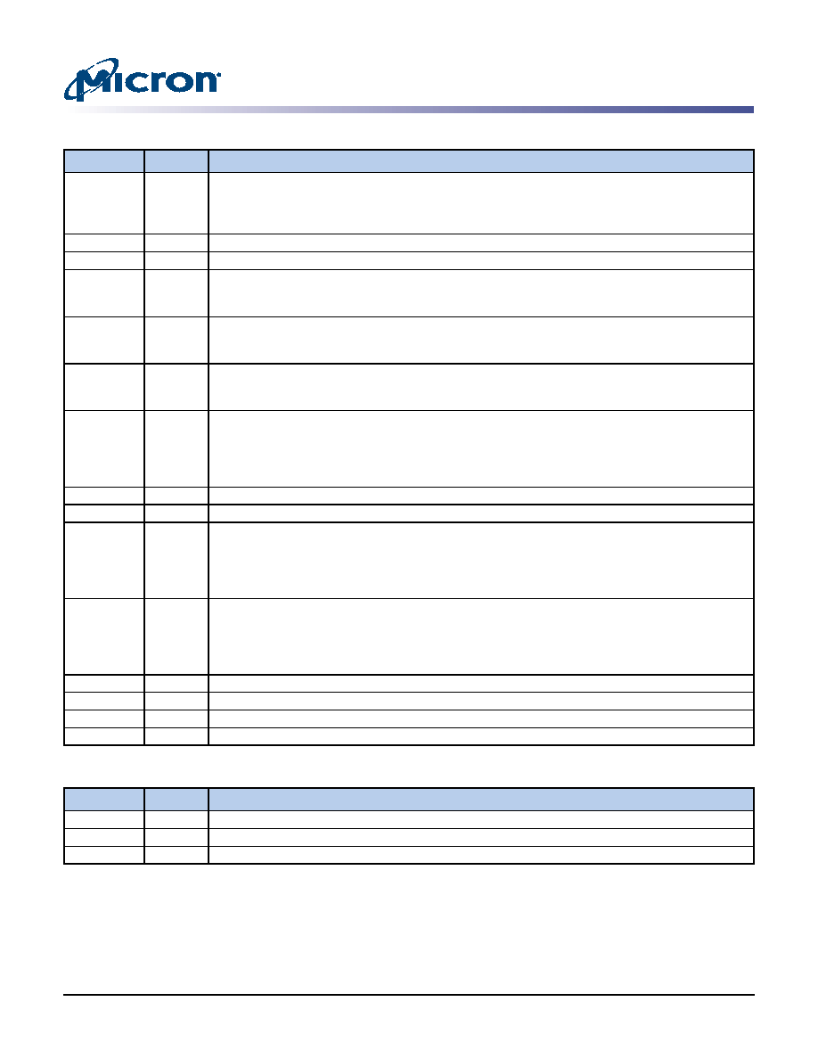
Table 3:
x16/x32 LPDDR Ball Descriptions
Symbol
Type
Description
A[14:0]
Input
Address inputs: Specifies the row or column address. Also used to load the mode registers. The
maximum LPDDR address is determined by density and configuration. Consult the LPDDR
product data sheet for the maximum address for a given density and configuration. Unused
address pins become RFU.
BA1, BA0
Input
Bank address inputs: Specifies one of the 4 banks.
CAS#
Input
Column select: Specifies the command to execute.
CK, CK#
Input
CK is the system clock. CK and CK# are differential clock inputs. All address and control signals
are sampled and referenced on the crossing of the rising edge of CK with the falling edge of
CK#.
CKE0, CKE1
Input
Clock enable:
CKE0 is used for a single LPDDR product.
CKE1 is used for dual LPDDR products.
CS1#, CS0#
Input
Chip select:
CS0# is used for a single LPDDR product.
CS1# is used for dual LPDDR products and is considered RFU for single LPDDR MCPs.
LDM, UDM
(x16)
DM[3:0]
(x32)
Input
Data mask: Determines which bytes are written during WRITE operations.
For x16 LPDDR, unused DM balls become RFU.
RAS#
Input
Row select: Specifies the command to execute.
WE#
Input
Write enable: Specifies the command to execute.
DQ[15:0]
(x16)
DQ[31:0]
(x32)
Input/
output
Data bus: Data inputs/outputs.
DQ[31:16] are RFU for x16 LPDDR devices.
LDQS, UDQS
(x16)
DQS[3:0]
(x32)
Input/
output
Data strobe: Coordinates READ/WRITE transfers of data; one DQS per DQ byte.
For x16 LPDDR, unused DQS balls become RFU.
TQ
Output
Temperature sensor output: TQ HIGH when LPDDR TJ exceeds 85°C.
VDD
Supply
VDD: LPDDR power supply.
VDDQ
Supply
VDDQ: LPDDR I/O power supply.
VSSQ
Supply
VSSQ: LPDDR I/O ground.
Table 4:
Non-Device-Specific Ball Descriptions
Symbol
Type
Description
VSS
Supply
VSS: Shared ground.
NC
–
No connect: Not internally connected.
RFU1
–
Reserved for future use.
相关PDF资料 |
PDF描述 |
|---|---|
| MT29F4G08BABWP | 512M X 8 FLASH 2.7V PROM, 18 ns, PDSO48 |
| MT36JSZF51272PDY-1G6XX | 512M X 72 DDR DRAM MODULE, DMA240 |
| MT3S04AU | UHF BAND, Si, NPN, RF SMALL SIGNAL TRANSISTOR |
| MT41J512M4JE-187EIT:A | 64M X 4 DDR DRAM, PBGA82 |
| MT42C8255RG-7TR | 256K X 8 VIDEO DRAM, 70 ns, PDSO40 |
相关代理商/技术参数 |
参数描述 |
|---|---|
| MT29C2G24MAKLAJA- 0 | 制造商:Micron Technology Inc 功能描述:128MX16/32MX32 MCP PLASTIC 1.8V COMBO - Trays |
| MT29C2G24MAKLAJA-6 IT | 制造商:Micron Technology Inc 功能描述:Combo Mem 128Mx16 Flash + 64Mx16 LPSDRAM 1.8V 168-Pin VFBGA Tray |
| MT29C2G24MAKLAJF-6 IT | 制造商:Micron Technology Inc 功能描述:128MX16/32MX32 MCP PLASTIC IND TEMP STACKED GREEN VFBGA 1.8V - Trays |
| MT29C2G24MAKLAJF-6 IT TR | 制造商:Micron Technology Inc 功能描述:128MX16/32MX32 MCP PLASTIC IND TEMP STACKED GREEN VFBGA 1.8V - Tape and Reel |
| MT29C2G24MAKLAJG-6 IT | 制造商:Micron Technology Inc 功能描述:Combo Mem 128Mx16 Flash + 32Mx32 LPSDRAM 1.8V 168-Pin VFBGA Tray 制造商:Micron Technology Inc 功能描述:128MX16/32MX32 MCP PLASTIC IND TEMP STACKED GREEN VFBGA 1.8V - Trays |
发布紧急采购,3分钟左右您将得到回复。