- 您现在的位置:买卖IC网 > PDF目录385639 > MT46V32M4-1 (Micron Technology, Inc.) DOUBLE DATA RATE DDR SDRAM PDF资料下载
参数资料
| 型号: | MT46V32M4-1 |
| 厂商: | Micron Technology, Inc. |
| 英文描述: | DOUBLE DATA RATE DDR SDRAM |
| 中文描述: | 双倍数据速率的DDR SDRAM内存 |
| 文件页数: | 17/68页 |
| 文件大小: | 2547K |
| 代理商: | MT46V32M4-1 |
第1页第2页第3页第4页第5页第6页第7页第8页第9页第10页第11页第12页第13页第14页第15页第16页当前第17页第18页第19页第20页第21页第22页第23页第24页第25页第26页第27页第28页第29页第30页第31页第32页第33页第34页第35页第36页第37页第38页第39页第40页第41页第42页第43页第44页第45页第46页第47页第48页第49页第50页第51页第52页第53页第54页第55页第56页第57页第58页第59页第60页第61页第62页第63页第64页第65页第66页第67页第68页
17
128Mb: x4, x8, x16 DDR SDRAM
128Mx4x8x16DDR_C.p65
–
Rev. C; Pub. 4/01
Micron Technology, Inc., reserves the right to change products or specifications without notice.
2001, Micron Technology, Inc.
128Mb: x4, x8, x16
DDR SDRAM
PRELIMINARY
READS
READ bursts are initiated with a READ command,
as shown in Figure 6.
The starting column and bank addresses are pro-
vided with the READ command and auto precharge is
either enabled or disabled for that burst access. If auto
precharge is enabled, the row being accessed is
precharged at the completion of the burst. For the
generic READ commands used in the following illus-
trations, auto precharge is disabled.
During READ bursts, the valid data-out element
from the starting column address will be available
following the CAS latency after the READ command.
Each subsequent data-out element will be valid nomi-
nally at the next positive or negative clock edge (i.e., at
the next crossing of CK and CK#). Figure 7 shows
general timing for each possible CAS latency setting.
DQS is driven by the DDR SDRAM along with output
data. The initial LOW state on DQS is known as the
read preamble; the LOW state coincident with the last
data-out element is known as the read postamble.
Upon completion of a burst, assuming no other
commands have been initiated, the DQs will go
High-Z. A detailed explanation of
t
DQSQ (valid data-
out skew),
t
QH (data-out window hold), the valid
data window are depicted in Figure 27. A detailed
explanation of
t
DQSCK (DQS transition skew to CK)
and
t
AC (data-out transition skew to CK) is depicted in
Figure 28.
Data from any READ burst may be concatenated
with or truncated with data from a subsequent READ
command. In either case, a continuous flow of data
can be maintained. The first data element from the new
burst follows either the last element of a completed
burst or the last desired data element of a longer burst
which is being truncated. The new READ command
should be issued
x
cycles after the first READ command,
where
x
equals the number of desired data element
pairs (pairs are required by the 2
n
-prefetch architec-
ture). This is shown in Figure 8. A READ command can
be initiated on any clock cycle following a previous
READ command. Nonconsecutive read data is shown
for illustration in Figure 9. Full-speed random read
accesses within a page (or pages) can be performed as
shown in Figure 10.
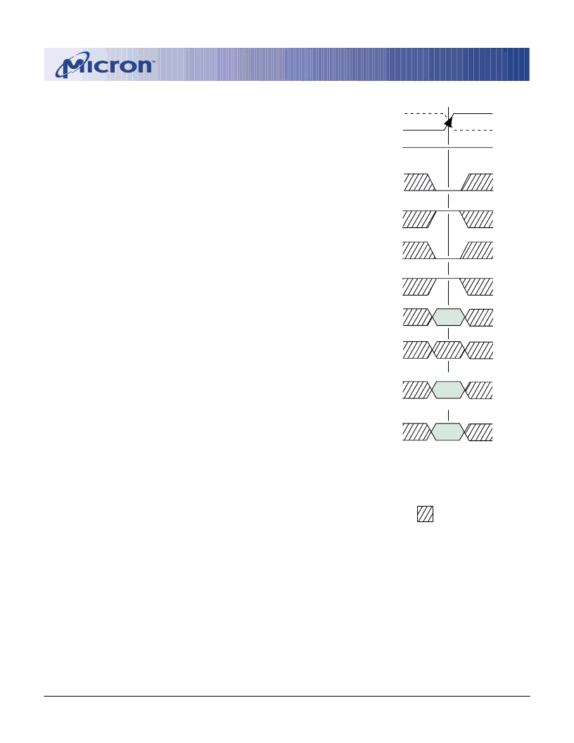
Figure 6
READ Command
CS#
WE#
CAS#
RAS#
CKE
CA
x4: A0
–
A9, A11
x8: A0
–
A9
x16: A0
–
A8
A10
BA0,1
HIGH
EN AP
DIS AP
BA
x8: A11
x16: A9, A11
CK
CK#
CA = Column Address
BA = Bank Address
EN AP = Enable Auto Precharge
DIS AP = Disable Auto Precharge
DON
’
T CARE
相关PDF资料 |
PDF描述 |
|---|---|
| MT46V32M4TG-75 | DOUBLE DATA RATE DDR SDRAM |
| MT46V32M4TG-75L | DOUBLE DATA RATE DDR SDRAM |
| MT46V32M4TG-75Z | DOUBLE DATA RATE DDR SDRAM |
| MT46V32M4TG-75ZL | DOUBLE DATA RATE DDR SDRAM |
| MT46V32M4TG-8 | DOUBLE DATA RATE DDR SDRAM |
相关代理商/技术参数 |
参数描述 |
|---|
发布紧急采购,3分钟左右您将得到回复。