- 您现在的位置:买卖IC网 > PDF目录385639 > MT46V32M4TG-8L (Micron Technology, Inc.) DOUBLE DATA RATE DDR SDRAM PDF资料下载
参数资料
| 型号: | MT46V32M4TG-8L |
| 厂商: | Micron Technology, Inc. |
| 英文描述: | DOUBLE DATA RATE DDR SDRAM |
| 中文描述: | 双倍数据速率的DDR SDRAM内存 |
| 文件页数: | 7/68页 |
| 文件大小: | 2547K |
| 代理商: | MT46V32M4TG-8L |
第1页第2页第3页第4页第5页第6页当前第7页第8页第9页第10页第11页第12页第13页第14页第15页第16页第17页第18页第19页第20页第21页第22页第23页第24页第25页第26页第27页第28页第29页第30页第31页第32页第33页第34页第35页第36页第37页第38页第39页第40页第41页第42页第43页第44页第45页第46页第47页第48页第49页第50页第51页第52页第53页第54页第55页第56页第57页第58页第59页第60页第61页第62页第63页第64页第65页第66页第67页第68页
7
128Mb: x4, x8, x16 DDR SDRAM
128Mx4x8x16DDR_C.p65
–
Rev. C; Pub. 4/01
Micron Technology, Inc., reserves the right to change products or specifications without notice.
2001, Micron Technology, Inc.
128Mb: x4, x8, x16
DDR SDRAM
PRELIMINARY
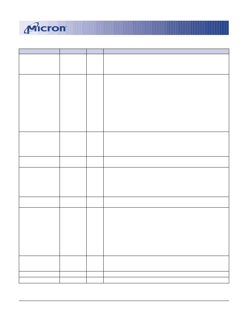
PIN DESCRIPTIONS
TSOP PIN NUMBERS
45, 46
SYMBOL
CK, CK#
TYPE
Input
DESCRIPTION
Clock: CK and CK# are differential clock inputs. All address and
control input signals are sampled on the crossing of the positive
edge of CK and negative edge of CK#. Output data (DQs and
DQS) is referenced to the crossings of CK and CK#.
Clock Enable: CKE HIGH activates and CKE LOW deactivates the
internal clock, input buffers and output drivers. Taking CKE LOW
provides PRECHARGE POWER-DOWN and SELF REFRESH
operations (all banks idle), or ACTIVE POWER-DOWN (row
ACTIVE in any bank). CKE is synchronous for POWER-DOWN
entry and exit, and for SELF REFRESH entry. CKE is asynchronous
for SELF REFRESH exit and for disabling the outputs. CKE must be
maintained HIGH throughout read and write accesses. Input
buffers (excluding CK, CK# and CKE) are disabled during POWER-
DOWN. Input buffers (excluding CKE) are disabled during SELF
REFRESH. CKE is an SSTL_2 input but will detect an LVCMOS
LOW level after V
DD
is applied.
Chip Select: CS# enables (registered LOW) and disables (regis-
tered HIGH) the command decoder. All commands are masked
when CS# is registered HIGH. CS# provides for external bank
selection on systems with multiple banks. CS# is considered part
of the command code.
Command Inputs: RAS#, CAS#, and WE# (along with CS#) define the
command being entered.
Input Data Mask: DM is an input mask signal for write data. Input
data is masked when DM is sampled HIGH along with that input data
during a WRITE access. DM is sampled on both edges of DQS.
Although DM pins are input-only, the DM loading is designed to
match that of DQ and DQS pins. For the x16 , LDM is DM for DQ0-
DQ7 and UDM is DM for DQ8-DQ15. Pin 20 is a NC on x4 and x8
Bank Address Inputs: BA0 and BA1 define to which bank an
ACTIVE, READ, WRITE, or PRECHARGE command is being applied.
Address Inputs: Provide the row address for ACTIVE commands, and
the column address and auto precharge bit (A10) for READ/WRITE
commands, to select one location out of the memory array in the
respective bank. A10 sampled during a PRECHARGE command
determines whether the PRECHARGE applies to one bank (A10 LOW,
bank selected by BA0, BA1) or all banks (A10 HIGH). The address
inputs also provide the op-code during a MODE REGISTER SET
command. BA0 and BA1 define which mode register (mode register
or extended mode register) is loaded during the LOAD MODE
REGISTER command.
Data Input/Output: Data bus for x16 (4, 7, 10, 13, 54, 57, 60, and 63
are NC for x8), (2, 4, 7, 8,10, 13, 54, 57, 59, 60, 63, and 65 are NC
for x4).
Data Input/Output: Data bus for x8 (2, 8, 59, and 65 are NC for x4).
Data Input/Output: Data bus for x4.
44
CKE
Input
24
CS#
Input
23, 22, 21
RAS#, CAS#,
WE#
DM
LDM, UDM
Input
47
Input
20, 47
26, 27
BA0, BA1
Input
29-32, 35-40,
28, 41
A0
–
A11
Input
2, 4, 5, 7, 8, 10,11, 13, 54
56, 57, 59, 60, 62, 63,65
DQ0
–
15
I/O
2, 5, 8, 11, 56, 59, 62, 65
5, 11, 56, 62
DQ0
–
7
DQ0
–
3
I/O
I/O
(continued on next page)
相关PDF资料 |
PDF描述 |
|---|---|
| MT46V4M32 | DOUBLE DATA RATE DDR SDRAM |
| MT46V4M32LG | I.MX31 LITE KIT |
| MT46V64M4 | 16 Meg x 4 x 4 banks DDR SDRAM(16M x 4 x 4组,双数据速率同步动态RAM) |
| MT46V64M8 | 16 Meg x 8 x 4 banks DDR SDRAM(16M x 8 x 4组,双数据速率同步动态RAM) |
| MT48LC16M8A1TG | SYNCHRONOUS DRAM |
相关代理商/技术参数 |
参数描述 |
|---|---|
| MT46V32M8 | 制造商:MICRON 制造商全称:Micron Technology 功能描述:DOUBLE DATA RATE DDR SDRAM |
| MT46V32M82ZZ5-75 ES | 制造商:Micron Technology Inc 功能描述:32MX8 SDRAM DDR PLASTIC PBF FBGA 2.5V - Trays |
| MT46V32M82ZZ5-75EZ | 制造商:Micron Technology Inc 功能描述:32MX8 DDR SDRAM PLASTIC 2.5V - Trays |
发布紧急采购,3分钟左右您将得到回复。