- 您现在的位置:买卖IC网 > PDF目录385639 > MT4LC1M16E5 (Micron Technology, Inc.) EDO DRAM PDF资料下载
参数资料
| 型号: | MT4LC1M16E5 |
| 厂商: | Micron Technology, Inc. |
| 英文描述: | EDO DRAM |
| 中文描述: | EDO公司的DRAM |
| 文件页数: | 1/24页 |
| 文件大小: | 385K |
| 代理商: | MT4LC1M16E5 |
1
1 Meg x 16 EDO DRAM
D52_B.p65 – Rev. B; Pub. 3/01
2001, Micron Technology, Inc
16Mb: 1 MEG x16
EDO DRAM
PRODUCTS AND SPECIFICATIONS DISCUSSED HEREIN ARE SUBJECT TO CHANGE BY MICRON WITHOUT NOTICE.
KEY TIMING PARAMETERS
SPEED
-5
-6
t
RC
84ns
104ns
t
RAC
50ns
60ns
t
PC
20ns
25ns
t
AA
25ns
30ns
t
CAC
15ns
17ns
t
CAS
8ns
10ns
FEATURES
JEDEC- and industry-standard x16 timing,
functions, pinouts, and packages
High-performance CMOS silicon-gate process
Single power supply (+3.3V ±0.3V or 5V ±10%)
All inputs, outputs and clocks are TTL-compatible
Refresh modes: RAS#-ONLY, CAS#-BEFORE-RAS#
(CBR), HIDDEN; optional self refresh (S)
BYTE WRITE access cycles
1,024-cycle refresh (10 row, 10 column addresses)
Extended Data-Out (EDO) PAGE MODE access
5V-tolerant inputs and I/Os on 3.3V devices
OPTIONS
Voltages
1
3.3V
5V
MARKING
LC
C
Refresh Addressing
1,024 (1K) rows
Packages
Plastic SOJ (400 mil)
Plastic TSOP (400 mil)
E5
DJ
TG
Timing
50ns access
60ns access
-5
-6
Refresh Rates
Standard Refresh (16ms period)
Self Refresh (128ms period)
None
S
2
Operating Temperature Range
Commercial (0
o
C to +70
o
C)
Extended (-20
o
C to +80
o
C)
None
ET
Part Number Example:
MT4LC1M16E5TG-6
NOTE:
1. The third field distinguishes the low voltage offering: LC desig-
nates Vcc = 3.3V and C designates Vcc = 5V.
2. Available only on MT4LC1M16E5 (3.3V)
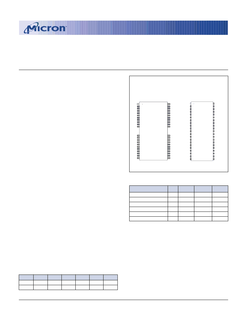
PIN ASSIGNMENT (Top View)
44/50-Pin TSOP
42-Pin SOJ
1 MEG x 16 EDO DRAM PART NUMBERS
PART NUMBER
MT4LC1M16E5DJ-x
MT4LC1M16E5DJ-x S
MT4LC1M16E5TG-x
MT4LC1M16E5TG-x S
MT4C1M16E5DJ-x
MT4C1M16E5TG-x
Vcc
3.3V
3.3V
3.3V
3.3V
5V
5V
REFRESH PACKAGE REFRESH
1K
400-SOJ
1K
400-SOJ
1K
400-TSOP
1K
400-TSOP
1K
400-SOJ
1K
400-TSOP
Standard
Self
Standard
Self
Standard
Standard
NOTE:
“ -x” indicates speed grade marking under timing
options.
EDO DRAM
MT4C1M16E5 – 1 Meg x 16, 5V
MT4LC1M16E5 – 1 Meg x 16, 3.3V
For the latest data sheet, please refer to the Micron Web
site:
www.micron.com/products/datasheets/sdramds.html
NOTE:
The "#" symbol indicates signal is active LOW.
V
CC
DQ0
DQ1
DQ3
V
CC
DQ4
DQ6
DQ7
NC
NC
NC
WE#
RAS#
NC
NC
A0
A1
A2
A3
V
CC
1
2
3
4
5
6
7
8
9
10
11
15
16
17
18
19
20
21
22
23
24
25
50
49
48
47
46
45
44
43
42
41
40
36
35
34
33
32
31
30
29
28
27
26
V
SS
DQ15
DQ14
DQ12
V
SS
DQ11
DQ9
DQ8
NC
NC
CASH#
OE#
A9
A8
A7
A6
A5
A4
V
SS
V
CC
DQ0
DQ1
DQ2
DQ3
V
CC
DQ4
DQ5
DQ6
DQ7
NC
NC
WE#
RAS#
NC
NC
A0
A1
A2
A3
V
CC
1
2
3
4
5
6
7
8
9
10
11
12
13
14
15
16
17
18
19
20
21
42
41
40
39
38
37
36
35
34
33
32
31
30
29
28
27
26
25
24
23
22
V
SS
DQ15
DQ14
DQ13
DQ12
V
SS
DQ11
DQ10
DQ9
DQ8
NC
CASL#
CASH#
OE#
A9
A8
A7
A6
A5
A4
V
SS
GENERAL DESCRIPTION
The 1 Meg x 16 is a randomly accessed, solid-state
memory containing 16,777,216 bits organized in a x16
configuration. The 1 Meg x 16 has both BYTE WRITE
and WORD WRITE access cycles via two CAS# pins
(CASL# and CASH#). These function like a single CAS#
found on other DRAMs in that either CASL# or CASH#
will generate an internal CAS#.
The CAS# function and timing are determined by
the first CAS# (CASL# or CASH#) to transition LOW and
the last CAS# to transition back HIGH. Using only one
相关PDF资料 |
PDF描述 |
|---|---|
| MT4C4256 | 256K x 4 DRAM Standard Or Low Power, Extended Refresh(标准或低功率,扩展刷新,256K x 4动态RAM) |
| MT4C4256L | 256K x 4 DRAM Standard Or Low Power, Extended Refresh(标准或低功率,扩展刷新,256K x 4动态RAM) |
| MT4LC16M4T8TG-5 | DRAM |
| MT4LC16M4T8TG-5S | DRAM |
| MT4LC16M4T8TG-6 | DRAM |
相关代理商/技术参数 |
参数描述 |
|---|---|
| MT4LC1M16E5DJ-5 | 制造商:MICRON 制造商全称:Micron Technology 功能描述:EDO DRAM |
| MT4LC1M16E5DJ-5S | 制造商:MICRON 制造商全称:Micron Technology 功能描述:EDO DRAM |
| MT4LC1M16E5DJ-6 | 制造商:MICRON 制造商全称:Micron Technology 功能描述:EDO DRAM |
| MT4LC1M16E5DJ-6S | 制造商:MICRON 制造商全称:Micron Technology 功能描述:EDO DRAM |
| MT4LC1M16E5TG-5 | 制造商:MICRON 制造商全称:Micron Technology 功能描述:EDO DRAM |
发布紧急采购,3分钟左右您将得到回复。