- 您现在的位置:买卖IC网 > PDF目录96090 > MTB33N10E (ON SEMICONDUCTOR) 33 A, 100 V, 0.06 ohm, N-CHANNEL, Si, POWER, MOSFET PDF资料下载
参数资料
| 型号: | MTB33N10E |
| 厂商: | ON SEMICONDUCTOR |
| 元件分类: | JFETs |
| 英文描述: | 33 A, 100 V, 0.06 ohm, N-CHANNEL, Si, POWER, MOSFET |
| 封装: | CASE 418B-03, D2PAK-3 |
| 文件页数: | 1/10页 |
| 文件大小: | 262K |
| 代理商: | MTB33N10E |
Semiconductor Components Industries, LLC, 2006
August, 2006 Rev. 4
1
Publication Order Number:
MTB33N10E/D
MTB33N10E
Preferred Device
Power MOSFET
33 Amps, 100 Volts
NChannel D2PAK
This Power MOSFET is designed to withstand high energy in the
avalanche and commutation modes. The energy efficient design also
offers a draintosource diode with a fast recovery time. Designed for
low voltage, high speed switching applications in power supplies,
converters and PWM motor controls, these devices are particularly
well suited for bridge circuits where diode speed and commutating
safe operating areas are critical and offer additional safety margin
against unexpected voltage transients.
Avalanche Energy Specified
SourcetoDrain Diode Recovery Time Comparable to a
Discrete Fast Recovery Diode
Diode is Characterized for Use in Bridge Circuits
IDSS and VDS(on) Specified at Elevated Temperature
Short Heatsink Tab Manufactured Not Sheared
Specially Designed Leadframe for Maximum Power Dissipation
MAXIMUM RATINGS (TC = 25°C unless otherwise noted)
Rating
Symbol
Value
Unit
DrainSource Voltage
VDSS
100
Vdc
DrainGate Voltage (RGS = 1.0 MΩ)
VDGR
100
Vdc
GateSource Voltage
Continuous
NonRepetitive (tp ≤ 10 ms)
VGS
VGSM
± 20
± 40
Vdc
Vpk
Drain Current Continuous
Drain Current Continuous @ 100°C
Drain Current Single Pulse (tp ≤ 10 μs)
ID
IDM
33
20
99
Adc
Apk
Total Power Dissipation
Derate above 25°C
Total Power Dissipation @ TA = 25°C,
when mounted with the minimum
recommended pad size
PD
125
1.0
2.5
Watts
W/°C
Watts
Operating and Storage Temperature
Range
TJ, Tstg
55 to
150
°C
Single Pulse DraintoSource Avalanche
Energy Starting TJ = 25°C
(VDD = 25 Vdc, VGS = 10 Vdc,
IL = 33 Apk, L = 1.000 mH, RG = 25 Ω)
EAS
545
mJ
Thermal Resistance
Junction to Case
Junction to Ambient
Junction to Ambient, when mounted
with the minimum recommended pad size
RθJC
RθJA
1.0
62.5
50
°C/W
Maximum Lead Temperature for Soldering
Purposes, 1/8″ from case for 10
seconds
TL
260
°C
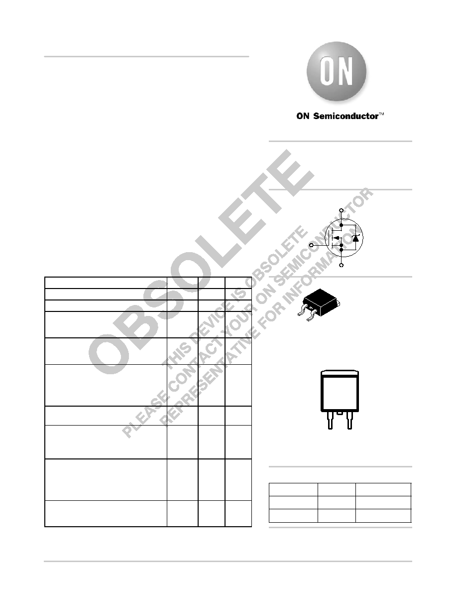
MARKING DIAGRAM
& PIN ASSIGNMENT
T33N10E
YWW
1
Gate
4
Drain
2
Drain
3
Source
33 AMPERES
100 VOLTS
RDS(on) = 60 mΩ
Device
Package
Shipping
ORDERING INFORMATION
MTB33N10E
D2PAK
50 Units/Rail
D2PAK
CASE 418B
STYLE 2
1
2
3
4
http://onsemi.com
NChannel
D
S
G
T33N10E
= Device Code
Y
= Year
WW
= Work Week
MTB33N10ET4
D2PAK
800/Tape & Reel
Preferred devices are recommended choices for future use
and best overall value.
相关PDF资料 |
PDF描述 |
|---|---|
| MTB33N10ET4 | 33 A, 100 V, 0.06 ohm, N-CHANNEL, Si, POWER, MOSFET |
| MTB35N06ZL | 35 A, 60 V, 0.026 ohm, N-CHANNEL, Si, POWER, MOSFET |
| MTB35N06ZLT4 | 35 A, 60 V, 0.026 ohm, N-CHANNEL, Si, POWER, MOSFET |
| MTB36N06VT4 | 32 A, 60 V, 0.04 ohm, N-CHANNEL, Si, POWER, MOSFET |
| MTB36N06VT4 | 32 A, 60 V, 0.04 ohm, N-CHANNEL, Si, POWER, MOSFET |
相关代理商/技术参数 |
参数描述 |
|---|---|
| MTB33N10ET4 | 制造商:ON Semiconductor 功能描述:Trans MOSFET N-CH 100V 33A 3-Pin(2+Tab) D2PAK T/R |
| MTB350W17-Q | 功能描述:TAG MKR BRASS RECT 3.5"X1.7" RoHS:否 类别:线缆,导线 - 管理 >> 标记 系列:Pan-Steel™ 标准包装:10 系列:- 类型:导线标记 - 套上式 尺寸:- 缆线直径:0.06" ~ 0.12"(1.5mm ~ 3.2mm) 图例:空白 颜色:白 材质:塑料 包装:每带 10 个;每包 1 条带 工作温度:- 其它名称:LBHZ2:SO/CMS |
| MTB36N06VT4 | 制造商:ON Semiconductor 功能描述:Trans MOSFET N-CH 60V 32A 3-Pin(2+Tab) D2PAK T/R |
| MTB3N120E | 制造商:ON Semiconductor 功能描述:Trans MOSFET N-CH 1.2KV 3A 3-Pin(2+Tab) D2PAK Rail |
| MTB3N120ET4 | 制造商:ON Semiconductor 功能描述:Trans MOSFET N-CH 1.2KV 3A 3-Pin(2+Tab) D2PAK T/R |
发布紧急采购,3分钟左右您将得到回复。