- 您现在的位置:买卖IC网 > PDF目录96090 > MTB33N10E (ON SEMICONDUCTOR) 33 A, 100 V, 0.06 ohm, N-CHANNEL, Si, POWER, MOSFET PDF资料下载
参数资料
| 型号: | MTB33N10E |
| 厂商: | ON SEMICONDUCTOR |
| 元件分类: | JFETs |
| 英文描述: | 33 A, 100 V, 0.06 ohm, N-CHANNEL, Si, POWER, MOSFET |
| 封装: | CASE 418B-03, D2PAK-3 |
| 文件页数: | 8/10页 |
| 文件大小: | 262K |
| 代理商: | MTB33N10E |
MTB33N10E
http://onsemi.com
7
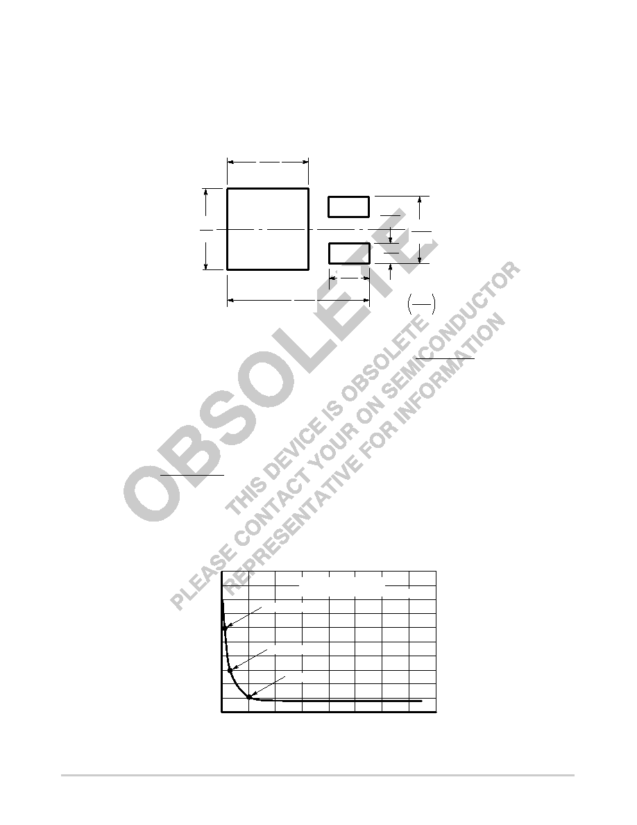
INFORMATION FOR USING THE D2PAK SURFACE MOUNT PACKAGE
RECOMMENDED FOOTPRINT FOR SURFACE MOUNTED APPLICATIONS
Surface mount board layout is a critical portion of the
total design. The footprint for the semiconductor packages
must be the correct size to ensure proper solder connection
interface between the board and the package. With the
correct pad geometry, the packages will self align when
subjected to a solder reflow process.
mm
inches
0.33
8.38
0.08
2.032
0.04
1.016
0.63
17.02
0.42
10.66
0.12
3.05
0.24
6.096
POWER DISSIPATION FOR A SURFACE MOUNT DEVICE
The power dissipation for a surface mount device is a
function of the drain pad size. These can vary from the
minimum pad size for soldering to a pad size given for
maximum power dissipation. Power dissipation for a
surface mount device is determined by TJ(max), the
maximum rated junction temperature of the die, RθJA, the
thermal resistance from the device junction to ambient, and
the operating temperature, TA. Using the values provided
on the data sheet, PD can be calculated as follows:
PD =
TJ(max) TA
RθJA
The values for the equation are found in the maximum
ratings table on the data sheet. Substituting these values
into the equation for an ambient temperature TA of 25°C,
one can calculate the power dissipation of the device. For a
D2PAK device, PD is calculated as follows.
PD = 150°C 25°C
50°C/W
= 2.5 Watts
The 50°C/W for the D2PAK package assumes the use of
the recommended footprint on a glass epoxy printed circuit
board to achieve a power dissipation of 2.5 Watts. There are
other alternatives to achieving higher power dissipation
from the surface mount packages. One is to increase the
area of the drain pad. By increasing the area of the drain
pad, the power dissipation can be increased. Although one
can almost double the power dissipation with this method,
one will be giving up area on the printed circuit board
which can defeat the purpose of using surface mount
technology. For example, a graph of RθJA versus drain pad
area is shown in Figure 16.
Figure 16. Thermal Resistance versus Drain Pad
Area for the D2PAK Package (Typical)
2.5 Watts
A, Area (square inches)
Board Material = 0.0625″
G10/FR4, 2 oz Copper
TA = 25°C
R
,
Thermal
Resistance,
Junction
to
Ambient
(C/W)
θ JA
°
60
70
50
40
30
20
16
14
12
10
8
6
4
2
0
3.5 Watts
5 Watts
相关PDF资料 |
PDF描述 |
|---|---|
| MTB33N10ET4 | 33 A, 100 V, 0.06 ohm, N-CHANNEL, Si, POWER, MOSFET |
| MTB35N06ZL | 35 A, 60 V, 0.026 ohm, N-CHANNEL, Si, POWER, MOSFET |
| MTB35N06ZLT4 | 35 A, 60 V, 0.026 ohm, N-CHANNEL, Si, POWER, MOSFET |
| MTB36N06VT4 | 32 A, 60 V, 0.04 ohm, N-CHANNEL, Si, POWER, MOSFET |
| MTB36N06VT4 | 32 A, 60 V, 0.04 ohm, N-CHANNEL, Si, POWER, MOSFET |
相关代理商/技术参数 |
参数描述 |
|---|---|
| MTB33N10ET4 | 制造商:ON Semiconductor 功能描述:Trans MOSFET N-CH 100V 33A 3-Pin(2+Tab) D2PAK T/R |
| MTB350W17-Q | 功能描述:TAG MKR BRASS RECT 3.5"X1.7" RoHS:否 类别:线缆,导线 - 管理 >> 标记 系列:Pan-Steel™ 标准包装:10 系列:- 类型:导线标记 - 套上式 尺寸:- 缆线直径:0.06" ~ 0.12"(1.5mm ~ 3.2mm) 图例:空白 颜色:白 材质:塑料 包装:每带 10 个;每包 1 条带 工作温度:- 其它名称:LBHZ2:SO/CMS |
| MTB36N06VT4 | 制造商:ON Semiconductor 功能描述:Trans MOSFET N-CH 60V 32A 3-Pin(2+Tab) D2PAK T/R |
| MTB3N120E | 制造商:ON Semiconductor 功能描述:Trans MOSFET N-CH 1.2KV 3A 3-Pin(2+Tab) D2PAK Rail |
| MTB3N120ET4 | 制造商:ON Semiconductor 功能描述:Trans MOSFET N-CH 1.2KV 3A 3-Pin(2+Tab) D2PAK T/R |
发布紧急采购,3分钟左右您将得到回复。