- 您现在的位置:买卖IC网 > PDF目录96090 > MTB3N100E (ON SEMICONDUCTOR) 3 A, 1000 V, 4 ohm, N-CHANNEL, Si, POWER, MOSFET PDF资料下载
参数资料
| 型号: | MTB3N100E |
| 厂商: | ON SEMICONDUCTOR |
| 元件分类: | JFETs |
| 英文描述: | 3 A, 1000 V, 4 ohm, N-CHANNEL, Si, POWER, MOSFET |
| 文件页数: | 6/10页 |
| 文件大小: | 262K |
| 代理商: | MTB3N100E |
MTB3N100E
5
Motorola TMOS Power MOSFET Transistor Device Data
16
QG, TOTAL GATE CHARGE (nC)
DRAIN–TO–SOURCE DIODE CHARACTERISTICS
VSD, SOURCE–TO–DRAIN VOLTAGE (VOLTS)
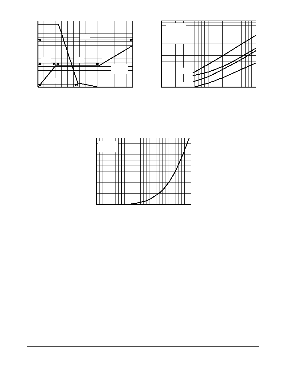
Figure 10. Diode Forward Voltage versus Current
I S
,SOURCE
CURRENT
(AMPS)
Figure 9. Resistive Switching Time
Variation versus Gate Resistance
RG, GATE RESISTANCE (OHMS)
1
10
100
1000
100
10
t,
TIME
(ns)
Figure 8. Gate–To–Source and Drain–To–Source
Voltage versus Total Charge
V
GS
,GA
TE–T
O–SOURCE
VOL
TAGE
(VOL
TS)
V
DS
,DRAIN–T
O–SOURCE
VOL
TAGE
(VOL
TS)
0
12
ID = 3 A
TJ = 25°C
VDS
VGS
Q1
Q2
QT
30
16
8
2
0
14
4
400
300
200
100
VDD = 500 V
ID = 3 A
VGS = 10 V
TJ = 25°C
0.50
0.70
0.78
0
3.0
0.66
0.74
0
0.80
0.58
0.54
0.62
2.5
1.0
Q3
4
20
28
2.0
1.5
0.5
12
10
6
350
250
150
50
8
24
VGS = 0 V
TJ = 25°C
td(on)
tf
td(off)
tr
SAFE OPERATING AREA
The Forward Biased Safe Operating Area curves define
the maximum simultaneous drain–to–source voltage and
drain current that a transistor can handle safely when it is for-
ward biased. Curves are based upon maximum peak junc-
tion temperature and a case temperature (TC) of 25°C. Peak
repetitive pulsed power limits are determined by using the
thermal response data in conjunction with the procedures
discussed in AN569, “Transient Thermal Resistance–General
Data and Its Use.”
Switching between the off–state and the on–state may tra-
verse any load line provided neither rated peak current (IDM)
nor rated voltage (VDSS) is exceeded and the transition time
(tr,tf) do not exceed 10 s. In addition the total power aver-
aged over a complete switching cycle must not exceed
(TJ(MAX) – TC)/(R
θJC).
A Power MOSFET designated E–FET can be safely used
in switching circuits with unclamped inductive loads. For reli-
able operation, the stored energy from circuit inductance dis-
sipated in the transistor while in avalanche must be less than
the rated limit and adjusted for operating conditions differing
from those specified. Although industry practice is to rate in
terms of energy, avalanche energy capability is not a con-
stant. The energy rating decreases non–linearly with an in-
crease of peak current in avalanche and peak junction
temperature.
Although many E–FETs can withstand the stress of drain–
to–source avalanche at currents up to rated pulsed current
(IDM), the energy rating is specified at rated continuous cur-
rent (ID), in accordance with industry custom. The energy rat-
ing must be derated for temperature as shown in the
accompanying graph (Figure 12). Maximum energy at cur-
rents below rated continuous ID can safely be assumed to
equal the values indicated.
相关PDF资料 |
PDF描述 |
|---|---|
| MTB3N100ET4 | 3 A, 1000 V, 4 ohm, N-CHANNEL, Si, POWER, MOSFET |
| MTB3N60E | 3 A, 600 V, 2.2 ohm, N-CHANNEL, Si, POWER, MOSFET |
| MTB4N80ET4 | 4 A, 800 V, 3 ohm, N-CHANNEL, Si, POWER, MOSFET |
| MTB50N06V | 42 A, 60 V, 0.028 ohm, N-CHANNEL, Si, POWER, MOSFET |
| MTB50N06VT4 | 42 A, 60 V, 0.028 ohm, N-CHANNEL, Si, POWER, MOSFET |
相关代理商/技术参数 |
参数描述 |
|---|---|
| MTB3N120E | 制造商:ON Semiconductor 功能描述:Trans MOSFET N-CH 1.2KV 3A 3-Pin(2+Tab) D2PAK Rail |
| MTB3N120ET4 | 制造商:ON Semiconductor 功能描述:Trans MOSFET N-CH 1.2KV 3A 3-Pin(2+Tab) D2PAK T/R |
| MTB3N60E | 制造商:Rochester Electronics LLC 功能描述:- Bulk 制造商:ON Semiconductor 功能描述: |
| MTB3N60ET4 | 制造商:Rochester Electronics LLC 功能描述:- Bulk 制造商:ON Semiconductor 功能描述: |
| MTB406N | 功能描述:拨动开关 4PDT TOGGLE SWITCH Decorat Bat Actuator RoHS:否 制造商:C&K Components 触点形式:DPDT 开关功能:ON - ON - ON 电流额定值: 电压额定值 AC:20 V 电压额定值 DC:20 V 功率额定值:0.4 VA 端接类型:V-Bracket 安装风格: 端子密封:Epoxy 触点电镀:Gold 照明:Not Illuminated |
发布紧急采购,3分钟左右您将得到回复。