- 您现在的位置:买卖IC网 > PDF目录187314 > MTP4N50E (ON SEMICONDUCTOR) 4 A, 500 V, 1.5 ohm, N-CHANNEL, Si, POWER, MOSFET, TO-220AB PDF资料下载
参数资料
| 型号: | MTP4N50E |
| 厂商: | ON SEMICONDUCTOR |
| 元件分类: | JFETs |
| 英文描述: | 4 A, 500 V, 1.5 ohm, N-CHANNEL, Si, POWER, MOSFET, TO-220AB |
| 文件页数: | 4/8页 |
| 文件大小: | 254K |
| 代理商: | MTP4N50E |
MTP4N50E
4
Motorola TMOS Power MOSFET Transistor Device Data
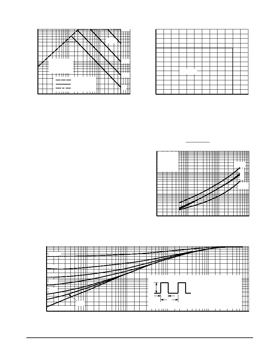
SAFE OPERATING AREA INFORMATION
I D
,DRAIN
CURRENT
(AMPS)
I D
,DRAIN
CURRENT
(AMPS)
VDS, DRAIN–TO–SOURCE VOLTAGE (VOLTS)
Figure 7. Maximum Rated Forward Biased
Safe Operating Area
VDS, DRAIN–TO–SOURCE VOLTAGE (VOLTS)
Figure 8. Maximum Rated Switching
Safe Operating Area
0
100
200
300
400
0
14
100
RDS(on) LIMIT
THERMAL LIMIT
PACKAGE LIMIT
10
VGS = 20 V
SINGLE PULSE
TC = 25°C
1
10
s
1 ms
10 ms
600
10
1
0.1
0.1 ms
TJ ≤ 150°C
1000
12
10
8
6
4
2
dc
500
FORWARD BIASED SAFE OPERATING AREA
The FBSOA curves define the maximum drain–to–source
voltage and drain current that a device can safely handle
when it is forward biased, or when it is on, or being turned on.
Because these curves include the limitations of simultaneous
high voltage and high current, up to the rating of the device,
they are especially useful to designers of linear systems. The
curves are based on a case temperature of 25
°C and a maxi-
mum junction temperature of 150
°C. Limitations for repetitive
pulses at various case temperatures can be determined by
using the thermal response curves. Motorola Application
Note, AN569, “Transient Thermal Resistance–General Data
and Its Use” provides detailed instructions.
SWITCHING SAFE OPERATING AREA
The switching safe operating area (SOA) of Figure 8 is the
boundary that the load line may traverse without incurring
damage to the MOSFET. The fundamental limits are the
peak current, IDM and the breakdown voltage, V(BR)DSS. The
switching SOA shown in Figure 8 is applicable for both turn–
on and turn–off of the devices for switching times less than
one microsecond.
The power averaged over a complete switching cycle must
be less than:
TJ(max) – TC
R
θJC
Figure 9. Resistive Switching Time
Variation versus Gate Resistance
t,
TIME
(ns)
RG, GATE RESISTANCE (OHMS)
VDD = 250 V
ID = 4 A
VGS = 10 V
TJ = 25°C
tf
td(off)
td(on)
1000
1
10000
10
100
1000
10
100
tr
Figure 10. Thermal Response
r(t)
,NORMALIZED
EFFECTIVE
TRANSIENT
THERMAL
RESIST
ANCE
R
θJC(t) = r(t) RθJC
R
θJC = 1.67°C/W MAX
D CURVES APPLY FOR POWER
PULSE TRAIN SHOWN
READ TIME AT t1
TJ(pk) – TC = P(pk) R
θJC(t)
P(pk)
t1
t2
DUTY CYCLE, D = t1/t2
t, TIME (ms)
1
0.01
0.2
D = 0.5
0.05
0.01
SINGLE PULSE
0.1
0.01
0.02
0.03
0.02
0.05
0.1
0.2
0.3
0.5
0.02
0.05
0.1
0.2
0.5
1
2
5
10
20
50
100
200
500
1000
相关PDF资料 |
PDF描述 |
|---|---|
| MTP60N10E7L | 60 A, 100 V, 0.024 ohm, N-CHANNEL, Si, POWER, MOSFET, TO-220AB |
| MTP71040L | 60 A, 100 V, 0.024 ohm, N-CHANNEL, Si, POWER, MOSFET, TO-220AB |
| MTP9N25E | 9 A, 250 V, 0.45 ohm, N-CHANNEL, Si, POWER, MOSFET, TO-220AB |
| MTSW-120-05-G-D-130 | 40 CONTACT(S), MALE, STRAIGHT BOARD STACKING CONNECTOR, SOLDER |
| MTSW-113-22-G-D-385 | 26 CONTACT(S), MALE, STRAIGHT BOARD STACKING CONNECTOR, SOLDER |
相关代理商/技术参数 |
参数描述 |
|---|---|
| MTP4N80 | 制造商:MOTOROLA 制造商全称:Motorola, Inc 功能描述:TMOS POWER FET 4.0 AMPERES 800 VOLTS RDS(on) = 3.0 OHM |
| MTP4N80E | 制造商:MOTOROLA 制造商全称:Motorola, Inc 功能描述:TMOS POWER FET 4.0 AMPERES 800 VOLTS RDS(on) = 3.0 OHM |
| MTP4N90 | 制造商:Motorola Inc 功能描述: |
| MTP4S-E10C | 制造商:Panduit Corp 功能描述:Mutiple Tie Plate, 4 Bundle, M-S Ties, # |
| MTP4S-E10-C | 功能描述:电缆束带 Mutiple Tie Plate, 4 Bundle, M-S Ties, # RoHS:否 制造商:Phoenix Contact 产品:Cable Tie Mounts 类型:Adhesive 颜色:Black 材料:Acrylonitrile Butadiene Styrene (ABS) 长度:19 mm 宽度:19 mm 抗拉强度: |
发布紧急采购,3分钟左右您将得到回复。