- 您现在的位置:买卖IC网 > PDF目录187314 > MTP4N50E (ON SEMICONDUCTOR) 4 A, 500 V, 1.5 ohm, N-CHANNEL, Si, POWER, MOSFET, TO-220AB PDF资料下载
参数资料
| 型号: | MTP4N50E |
| 厂商: | ON SEMICONDUCTOR |
| 元件分类: | JFETs |
| 英文描述: | 4 A, 500 V, 1.5 ohm, N-CHANNEL, Si, POWER, MOSFET, TO-220AB |
| 文件页数: | 5/8页 |
| 文件大小: | 254K |
| 代理商: | MTP4N50E |
MTP4N50E
5
Motorola TMOS Power MOSFET Transistor Device Data
GATE–TO–SOURCE OR DRAIN–TO–SOURCE VOLTAGE (VOLTS)
Figure 11. Capacitance Variation
C,
CAP
ACIT
ANCE
(pF)
VGS
VDS
VDS = 0
0
Ciss
Coss
Crss
2000
1500
1000
25
20
10
0
5
10
Figure 12. Gate Charge versus
Gate–To–Source Voltage
QG, TOTAL GATE CHARGE (nC)
16
0
20
12
8
4
30
40
50
5
15
500
VDS = 100 V
V
GS
,GA
TE
SOURCE
VOL
TAGE
(VOL
TS)
TJ = 25°C
ID = 4 A
400 V
250 V
TJ = 25°C
VGS = 0
10
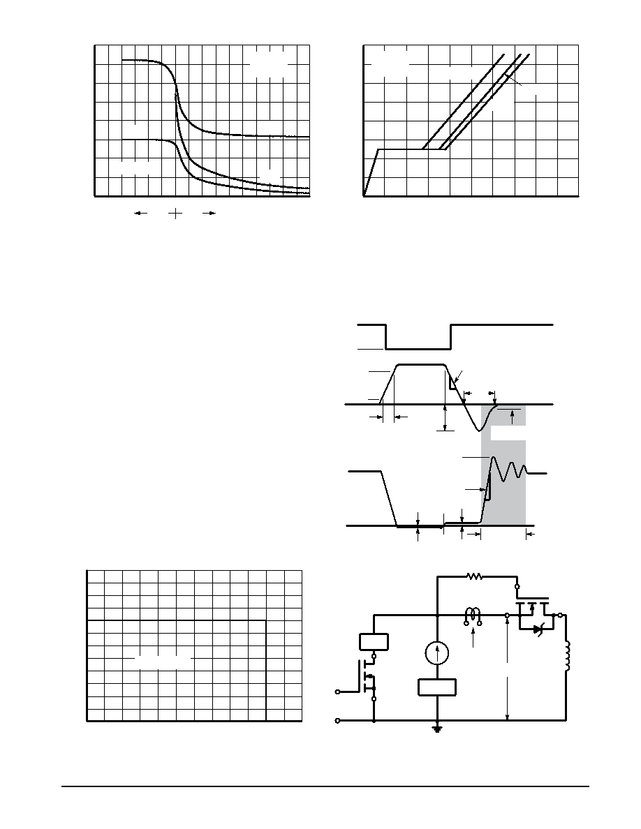
COMMUTATING SAFE OPERATING AREA (CSOA)
The Commutating Safe Operating Area (CSOA) of
Figure 14 defines the limits of safe operation for commutated
source–drain current versus re–applied drain voltage when
the source–drain diode has undergone forward bias. The
curve shows the limitations of IFM and peak VDS for a given
rate of change of source current. It is applicable when wave-
forms similar to those of Figure 13 are present. Full or half–
bridge PWM DC motor controllers are common applications
requiring CSOA data.
Device stresses increase with increasing rate of change of
source current so dIs/dt is specified with a maximum value.
Higher values of dIs/dt require an appropriate derating of IFM,
peak VDS or both. Ultimately dIs/dt is limited primarily by de-
vice, package, and circuit impedances. Maximum device
stress occurs during trr as the diode goes from conduction to
reverse blocking.
VDS(pk) is the peak drain–to–source voltage that the device
must sustain during commutation; IFM is the maximum for-
ward source–drain diode current just prior to the onset of
commutation.
VR is specified at 80% of V(BR)DSS to ensure that the
CSOA stress is maximized as IS decays from IRM to zero.
RGS should be minimized during commutation. TJ has only
a second order effect on CSOA.
Stray inductances in Motorola’s test circuit are assumed to
be practical minimums. dVDS/dt in excess of 10 V/ns was at-
tained with dIs/dt of 400 A/s.
I D
,DRAIN
CURRENT
(AMPS)
Figure 13. Commutating Safe Operating Area (CSOA)
0
100
200
300
400
6
4
2
0
VDS, DRAIN–TO–SOURCE VOLTAGE (VOLTS)
+
–
Figure 14. Commutating Safe Operating Area
Test Circuit
VR
VGS
IFM
20 V
RGS
DUT
IS
Li
VR = 80% OF RATED VDS
VdsL = Vf + Li dls/dt
+
–
di/dt
≤ 75 A/s
500
VDS
600
Figure 15. Commutating Waveforms
15 V
VGS
0
90%
IFM
dls/dt
IS
10%
trr
IRM
ton
VDS
Vf
VdsL
dVDS/dt
VDS(pk)
MAX. CSOA
STRESS AREA
VR
0.25 IRM
相关PDF资料 |
PDF描述 |
|---|---|
| MTP60N10E7L | 60 A, 100 V, 0.024 ohm, N-CHANNEL, Si, POWER, MOSFET, TO-220AB |
| MTP71040L | 60 A, 100 V, 0.024 ohm, N-CHANNEL, Si, POWER, MOSFET, TO-220AB |
| MTP9N25E | 9 A, 250 V, 0.45 ohm, N-CHANNEL, Si, POWER, MOSFET, TO-220AB |
| MTSW-120-05-G-D-130 | 40 CONTACT(S), MALE, STRAIGHT BOARD STACKING CONNECTOR, SOLDER |
| MTSW-113-22-G-D-385 | 26 CONTACT(S), MALE, STRAIGHT BOARD STACKING CONNECTOR, SOLDER |
相关代理商/技术参数 |
参数描述 |
|---|---|
| MTP4N80 | 制造商:MOTOROLA 制造商全称:Motorola, Inc 功能描述:TMOS POWER FET 4.0 AMPERES 800 VOLTS RDS(on) = 3.0 OHM |
| MTP4N80E | 制造商:MOTOROLA 制造商全称:Motorola, Inc 功能描述:TMOS POWER FET 4.0 AMPERES 800 VOLTS RDS(on) = 3.0 OHM |
| MTP4N90 | 制造商:Motorola Inc 功能描述: |
| MTP4S-E10C | 制造商:Panduit Corp 功能描述:Mutiple Tie Plate, 4 Bundle, M-S Ties, # |
| MTP4S-E10-C | 功能描述:电缆束带 Mutiple Tie Plate, 4 Bundle, M-S Ties, # RoHS:否 制造商:Phoenix Contact 产品:Cable Tie Mounts 类型:Adhesive 颜色:Black 材料:Acrylonitrile Butadiene Styrene (ABS) 长度:19 mm 宽度:19 mm 抗拉强度: |
发布紧急采购,3分钟左右您将得到回复。